Basic topology and parameter design and introduction of amplifier
Traditional RF amplifiers use discrete transistor active devices, mainly because of the low cost of the device. With the improvement of the performance of the op amp and the promotion of batch applications, the use of op amps in RF amplifiers has become a trend. Compared with discrete transistors, high-speed op amps do have their advantages: First, the former constitutes an amplifier whose gain and bandwidth have a large relationship with the bias current and operating point of the transistor, making it relatively difficult to adjust; and the gain of the op amp is not biased. Affected. Second, the op amp can also reduce parameter drift over the operating temperature range, making the job more reliable and stable.
As we all know, the op amp can be divided into voltage feedback type (VFB) and current feedback type (CFB). In practical applications, VFB op amps are used in large quantities, but in RF amplifier applications, CFB op amps have better performance. The gain-bandwidth product of the VFB op amp is constant, and the gain is limited by the bandwidth; the CFB is still at a higher gain near the highest frequency. For example, the open-loop bandwidth (-3dB) of the VFB op amp THS4001 is 270MHz, the available bandwidth is only 10MHz when the gain is 100 (20dB), and the open-band bandwidth (-3dB) of the CFB op amp THS3001 is 420MHz. Up to 150MHz.
Of course, RF designers also need to understand some of the features of CFB op amps:
• The internal structure of the amplifier's op amp is different, but the basic topology that makes up the amplifier has not changed.
• The feedback resistor RF value recommended by the CFB op amp data sheet should be strictly observed, and the gain should be adjusted by applying RG.
• There must be no capacitors in the feedback loop.
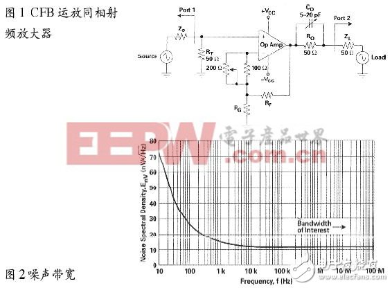
Basic topology and parameters of the amplifierThe basic topology of the CFB op amp RF amplifier is still the structure of the feedback amplifier, which has two forms of non-inverting amplifier and inverting amplifier. On the other hand, for the RF circuit, pay special attention to the impedance matching between the input and the output. The system is usually connected with a 50Ω cable. Since the input impedance of the op amp is high, the input is connected with a 50Ω resistor. At the output, the output is The output impedance is low, so a 50Ω resistor is connected in series. Thus, the non-inverting amplifier is shown in Figure 1.
RF circuit performance is typically characterized by four scattering (S) parameters. The term "scattering" implies the meaning of loss. The reflection, ie the scattering parameters S11 and S12, reduces the useful signal, the reverse transmission S12 returns the output power from the load, and only the positive transmission S21 is a useful scattering parameter. Designing the RF circuit is to reduce S11, S22 and S12 and increase S21. The small-signal AC parameters of the RF amplifier can be derived from the S-parameter. The relationship between the two is shown in Table 1. These indicators are frequency dependent.
The input-to-output voltage standing wave ratio (VSWR) is a ratio and is therefore a unitless quantity. It is a measure of the matching of the input and output impedances with the source impedance and the load impedance. To avoid reflections, the matching should be as close as possible. VSWR is defined as:
VSWR=Z(I/O)/ZS or ZS/Z(I/O)
The ideal VSWR is equal to 1:1, however the typical VSWR will not be better than 1.5:1 over the operating frequency range. The input and output impedance of the op amp are determined by the external components selected by the designer, so the op amp's data sheet does not specify the VSWR. Return Loss—The relationship between this value and VSWR is:
Return loss = 20log (VSWR + 1) / (VSWR - 1)
=10log(s11)2 (input)
=10log(S22)2 (output)
Since the output impedance is not exactly matched to ZL at the RF, it gradually increases as the loop gain decreases, so the RO is shunted in parallel to compensate.
The forward transmission S21 is determined by the input resistor RG and the feedback resistor RF, and is expressed to the in-phase type operational amplifier S21 as:
S21=AL=1/2(1+RF/RG)
Note that a series resistor is added to the output and the voltage divider reduces the gain by half. For RF amplification, the usual power gain is used to indicate:
PO (dBm) = 10log (absolute power / 0.001W)
dBm=dBV+13 (50Ω termination resistance)
The reverse transmission S12 indicates the isolation between the input and the output. The isolation of the CFB RF op amp is quite good, especially for the non-inverting amplifier. Its feedback is connected to the inverting terminal to make the isolation better.
Phase Linearity—Designers often care about the phase response of RF circuits. The phase linearity of CFB amplifiers is better than VFB amplifiers, such as:
VFB THS4001 has a differential phase shift of 0.15°
The differential phase shift of CFB THS3001 is 0.02°
Frequency Response Flatness - The CFB amplifier can adjust the flatness of the frequency response without affecting the forward gain by trimming the resistor (see the resistor in series with the inverting terminal of Figure 1). Coupled with the trimming resistor, the RF and RG values ​​are reduced accordingly, but their ratio remains the same and the gain remains the same.
-1dB compression point - The -1dB compression point is defined as: At a fixed frequency, the actual power of the amplifier is 1dB less than expected. In other words, the amplifier gain is reduced by 1dB compared to low power. The -1dB compression point is a representation of the RF rail value by the RF designer. RF designers are more concerned with maximizing gain. A slight clamp is allowed. As long as the generated harmonics are within the scope of the relevant regulations, a -1dB compression point is determined.
The standard AC-coupled RF amplifier exhibits a relatively constant -1dB compression point over the operating frequency range. At low frequencies, increasing the power at a fixed frequency will eventually drive the output to the rail value, the VOM specification; at high frequencies, the op amp will be limited by the slew rate, and the slew rate will be reduced by half because the output uses a matching resistor.
High-speed Board-to-board Connectors
High-Speed Board-To-Board Connectors,8 Mm High Board-To-Board Connectors,Pin 10-120Pin Board-To-Board Connectors,High Speed 14Gbps Board-To-Board Connectors
Dongguan SOLEPIN Electronics Co., Ltd , https://www.wentae.com