Conversion between clock jitter (CLK) and phase noise
Abstract: This is an application note on clock (CLK) signal quality that describes how to measure jitter and phase noise, including periodic jitter, cycle-by-cycle jitter, and cumulative jitter. This article also describes the relationship between periodic jitter and phase noise spectrum, and describes how to convert the phase noise spectrum into periodic jitter.
Almost all integrated circuits and electrical systems require a clock (CLK). In today's world, people process and transmit digital information at a faster rate, and the conversion rate between analog signals and digital signals is getting faster and faster, and the resolution is getting higher and higher. All these require engineers to pay more attention to the quality of the clock signal.
The quality of the clock signal is usually described by jitter and phase noise. Jitter includes periodic jitter, cycle-by-cycle jitter and cumulative jitter. The most commonly used is jitter. The phase noise of the clock is used to illustrate the spectral characteristics of the clock signal.
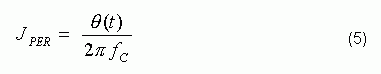
This article first briefly introduces the devices used to measure clock jitter and phase noise. Then introduce the relationship between periodic jitter and phase noise, and finally introduce a simple formula to convert the phase noise spectrum into periodic jitter. Period jitter and phase noise: Define and measure period jitter Period jitter (JPER) is the time difference between the measured period and the ideal period. Due to the characteristics of random distribution, it can be described by peak-to-peak or root mean square (RMS). We first define TPER (n), whose threshold is the clock rising edge of VTH, in the time domain, where n is a time domain coefficient, as shown in Figure 1. We express JPER as a manual:
Where TO is the ideal clock period. Since the clock frequency is fixed, the mean value of random jitter JPER should be zero, and the RMS of JPER can be expressed as:

<In the formula![]() > Is the required operator. From the clock waveform in Figure 1, you can see the relationship between JPER and TPER.
> Is the required operator. From the clock waveform in Figure 1, you can see the relationship between JPER and TPER.
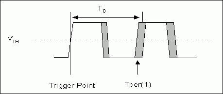
Figure 1. Period jitter measurement
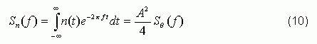
Phase noise measurement In order to understand the definition of the phase noise spectrum L (f), we first define the power spectral density SC (f) of the clock signal. Connect the clock signal to the spectrum analyzer to measure SC (f). The phase noise spectrum L (f) is defined as the difference between the SC (f) value at the frequency f and the SC (f) value at the clock frequency fC, expressed in dB. Figure 2 illustrates the definition of L (f).
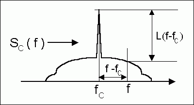
Figure 2. Definition of the phase noise spectrum
The mathematical definition of the phase noise spectrum L (f) is:

Note that L (f) represents the ratio of the spectral values ​​at fC and f, and L (f) will be described below.
Periodic jitter (JPER) measurement There are many devices that can measure periodic jitter. Usually people will use high precision digital oscilloscope to measure jitter. When the clock jitter is greater than 5 times the oscilloscope trigger jitter, the clock jitter can be triggered by the rising edge of the clock, and then measure another rising edge. Figure 3 shows how the oscilloscope generates a trigger signal from the clock under test. This method can eliminate the internal clock source jitter of the digital oscilloscope.
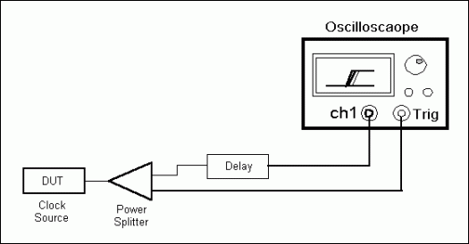
Figure 3. Self-triggered jitter measurement device
The trigger delay of the oscilloscope may be greater than one high-frequency clock cycle. Therefore, a delay element must be added to the signal path to display the first rising edge triggered on the screen.
Of course, there are some more accurate jitter measurement methods, but most of them post-process the data collected by the high-speed digital oscilloscope, and calculate the jitter according to the definition of formula 1 or 2. Post-processing can get more accurate results, but high-end digital oscilloscopes are required [2, 3].
The phase noise spectrum L (f) measurement is shown in Equation 3. L (f) can be obtained by directly measuring the spectrum SC (f) of the clock signal through a spectrum analyzer. But in fact, because L (f) is usually greater than 100dBc, which exceeds the dynamic range of most spectrum analyzers, this method is not realistic. In addition, fC sometimes exceeds the input frequency limit of the spectrum analyzer. In fact, the device measuring phase noise needs to filter out the spectral energy of fC. This method is similar to demodulating the passband signal to baseband. Fig. 4 is an actual phase noise measurement device and the spectrum conversion at different positions.
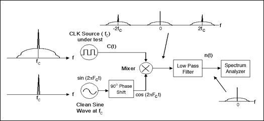
Figure 4. Actual noise spectrum measurement device
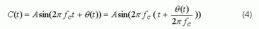
The architecture shown in Figure 4 is commonly referred to as a carrier suppression demodulator, and n (t) in Figure 4 is the spectrum analyzer input. We can obtain the dBc value of L (f) by adjusting the n (t) spectrum correctly. The relationship between the root mean square value of the period jitter and the phase noise can be seen through the Fourier series, and the jitter characteristics of the clock square wave signal and its fundamental frequency sine wave signal are basically the same. This greatly simplifies the jitter analysis of the clock signal. A sine wave clock signal with phase noise can be described as:
The period jitter can be expressed as:
Equation 4 shows that the sine wave has undergone phase noise Θ (t) phase modulation. Since the phase noise is much smaller than π / 2, Equation 4 can be simplified to:
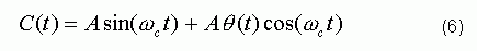
The spectrum C (t) can be expressed as:

Where SΘ (f) is the frequency domain representation of q (t). According to the definition of L (f), we can get:

It can be seen that L (f) is SΘ (f) expressed in dB. This actually reveals the true meaning of L (f).
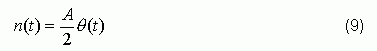
Through the device shown in Figure 4, L (f), C (t) and cos (2Ï€fCt) can be mixed, filtered by a low-pass filter, and then input into the spectrum analyzer.
The output of the spectrum analyzer is:
From this, phase noise SΘ (f) and L (f) can be obtained:
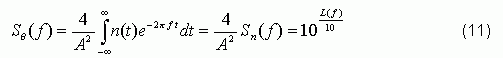
By scaling down the spectrum of n (t) by A² / 4, you can directly get L (f) expressed in dBc.
The mean square value (MS) of Θ (t) can be derived by Equation 11:
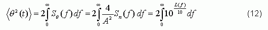
Starting from Equation 5, the relationship between period jitter and phase noise spectrum L (f) is finally derived:
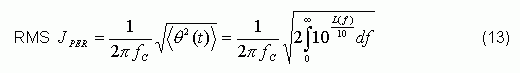
In some similar SONET and 10Gb applications, engineers only care about jitter in specific frequency bands. The RMS JPER in a specific frequency band can be expressed as:
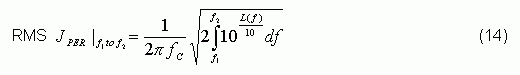 RMS JPER can be obtained by L (f) approximation. When L (f) frequency axis is logarithmic, phase noise can usually be approximated by piecewise linear method. L (f) at this time can be expressed as:
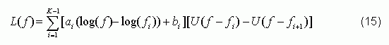
Where K-1 is the number of line segments of the piecewise function, and U (f) is the step function, as shown in Figure 5:
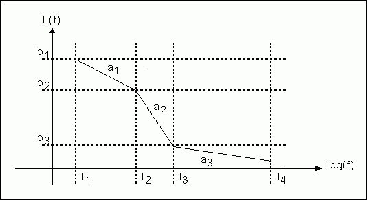
Figure 5. A typical L (f) function
Taking L (f) in Equation 15 into Equation 14, we can get:
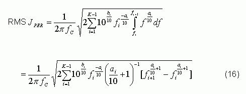
Table 1 is the L (f) list of fC = 155.52MHz, which can be used for the calculation of the piecewise function parameters.
Table 1. L (f) values ​​used to calculate the parameters of the piecewise function
The following calculates ai and bi:

The results are shown in Table 2.
Table 2. Parameters in the L (f) piecewise function
Taking the values ​​in Table 2 into Equation 16, we can get:

Using the device shown in Figure 4, the RMS jitter of the same clock in the same frequency band is 4.2258ps, so the approximate conversion result from phase noise to jitter is very accurate. The error in this example is less than 4%.
Given the envelope of the phase noise spectrum, Equation 16 can also be used to estimate the upper limit of jitter required. Summary This article reveals the mathematical relationship between jitter measured in the time domain and phase noise measured in the frequency domain. Many engineers who care about signal integrity and system clock will pay attention to this relationship. The results of this article clearly answer this question. Based on the above mathematical relationship, we propose a method to estimate the period jitter using the phase noise spectrum. Engineers can use this method to quickly achieve quantitative conversion between the two measurements, which is very helpful for the design and application of system circuits.
Almost all integrated circuits and electrical systems require a clock (CLK). In today's world, people process and transmit digital information at a faster rate, and the conversion rate between analog signals and digital signals is getting faster and faster, and the resolution is getting higher and higher. All these require engineers to pay more attention to the quality of the clock signal.
The quality of the clock signal is usually described by jitter and phase noise. Jitter includes periodic jitter, cycle-by-cycle jitter and cumulative jitter. The most commonly used is jitter. The phase noise of the clock is used to illustrate the spectral characteristics of the clock signal.
This article first briefly introduces the devices used to measure clock jitter and phase noise. Then introduce the relationship between periodic jitter and phase noise, and finally introduce a simple formula to convert the phase noise spectrum into periodic jitter. Period jitter and phase noise: Define and measure period jitter Period jitter (JPER) is the time difference between the measured period and the ideal period. Due to the characteristics of random distribution, it can be described by peak-to-peak or root mean square (RMS). We first define TPER (n), whose threshold is the clock rising edge of VTH, in the time domain, where n is a time domain coefficient, as shown in Figure 1. We express JPER as a manual:
Where TO is the ideal clock period. Since the clock frequency is fixed, the mean value of random jitter JPER should be zero, and the RMS of JPER can be expressed as:
<In the formula
Figure 1. Period jitter measurement
Phase noise measurement In order to understand the definition of the phase noise spectrum L (f), we first define the power spectral density SC (f) of the clock signal. Connect the clock signal to the spectrum analyzer to measure SC (f). The phase noise spectrum L (f) is defined as the difference between the SC (f) value at the frequency f and the SC (f) value at the clock frequency fC, expressed in dB. Figure 2 illustrates the definition of L (f).
Figure 2. Definition of the phase noise spectrum
The mathematical definition of the phase noise spectrum L (f) is:
Note that L (f) represents the ratio of the spectral values ​​at fC and f, and L (f) will be described below.
Periodic jitter (JPER) measurement There are many devices that can measure periodic jitter. Usually people will use high precision digital oscilloscope to measure jitter. When the clock jitter is greater than 5 times the oscilloscope trigger jitter, the clock jitter can be triggered by the rising edge of the clock, and then measure another rising edge. Figure 3 shows how the oscilloscope generates a trigger signal from the clock under test. This method can eliminate the internal clock source jitter of the digital oscilloscope.
Figure 3. Self-triggered jitter measurement device
The trigger delay of the oscilloscope may be greater than one high-frequency clock cycle. Therefore, a delay element must be added to the signal path to display the first rising edge triggered on the screen.
Of course, there are some more accurate jitter measurement methods, but most of them post-process the data collected by the high-speed digital oscilloscope, and calculate the jitter according to the definition of formula 1 or 2. Post-processing can get more accurate results, but high-end digital oscilloscopes are required [2, 3].
The phase noise spectrum L (f) measurement is shown in Equation 3. L (f) can be obtained by directly measuring the spectrum SC (f) of the clock signal through a spectrum analyzer. But in fact, because L (f) is usually greater than 100dBc, which exceeds the dynamic range of most spectrum analyzers, this method is not realistic. In addition, fC sometimes exceeds the input frequency limit of the spectrum analyzer. In fact, the device measuring phase noise needs to filter out the spectral energy of fC. This method is similar to demodulating the passband signal to baseband. Fig. 4 is an actual phase noise measurement device and the spectrum conversion at different positions.
Figure 4. Actual noise spectrum measurement device
The architecture shown in Figure 4 is commonly referred to as a carrier suppression demodulator, and n (t) in Figure 4 is the spectrum analyzer input. We can obtain the dBc value of L (f) by adjusting the n (t) spectrum correctly. The relationship between the root mean square value of the period jitter and the phase noise can be seen through the Fourier series, and the jitter characteristics of the clock square wave signal and its fundamental frequency sine wave signal are basically the same. This greatly simplifies the jitter analysis of the clock signal. A sine wave clock signal with phase noise can be described as:
The period jitter can be expressed as:
Equation 4 shows that the sine wave has undergone phase noise Θ (t) phase modulation. Since the phase noise is much smaller than π / 2, Equation 4 can be simplified to:
The spectrum C (t) can be expressed as:
Where SΘ (f) is the frequency domain representation of q (t). According to the definition of L (f), we can get:
It can be seen that L (f) is SΘ (f) expressed in dB. This actually reveals the true meaning of L (f).
Through the device shown in Figure 4, L (f), C (t) and cos (2Ï€fCt) can be mixed, filtered by a low-pass filter, and then input into the spectrum analyzer.
The output of the spectrum analyzer is:
From this, phase noise SΘ (f) and L (f) can be obtained:
By scaling down the spectrum of n (t) by A² / 4, you can directly get L (f) expressed in dBc.
The mean square value (MS) of Θ (t) can be derived by Equation 11:
Starting from Equation 5, the relationship between period jitter and phase noise spectrum L (f) is finally derived:
In some similar SONET and 10Gb applications, engineers only care about jitter in specific frequency bands. The RMS JPER in a specific frequency band can be expressed as:
RMS JPER can be obtained by L (f) approximation. When L (f) frequency axis is logarithmic, phase noise can usually be approximated by piecewise linear method. L (f) at this time can be expressed as: Where K-1 is the number of line segments of the piecewise function, and U (f) is the step function, as shown in Figure 5:
Figure 5. A typical L (f) function
Taking L (f) in Equation 15 into Equation 14, we can get:
Table 1 is the L (f) list of fC = 155.52MHz, which can be used for the calculation of the piecewise function parameters.
Table 1. L (f) values ​​used to calculate the parameters of the piecewise function
| Frequency (Hz) | 10 | 1000 | 3000 | 10000 |
| L (f) (dBc) | -58 | -118 | -132 | -137 |
The following calculates ai and bi:
The results are shown in Table 2.
Table 2. Parameters in the L (f) piecewise function
| i | 1 | 2 | 3 | 4 |
| fi (Hz) | 10 | 1000 | 3000 | 10000 |
| ai (dBc / decade) | -30 | -29.34 | -9.5 | N / A |
| bi (dBc) | -58 | -118 | -132 | -137 |
Taking the values ​​in Table 2 into Equation 16, we can get:
Using the device shown in Figure 4, the RMS jitter of the same clock in the same frequency band is 4.2258ps, so the approximate conversion result from phase noise to jitter is very accurate. The error in this example is less than 4%.
Given the envelope of the phase noise spectrum, Equation 16 can also be used to estimate the upper limit of jitter required. Summary This article reveals the mathematical relationship between jitter measured in the time domain and phase noise measured in the frequency domain. Many engineers who care about signal integrity and system clock will pay attention to this relationship. The results of this article clearly answer this question. Based on the above mathematical relationship, we propose a method to estimate the period jitter using the phase noise spectrum. Engineers can use this method to quickly achieve quantitative conversion between the two measurements, which is very helpful for the design and application of system circuits.
Over time, battery cables have to be replaced due to corrosion or damage. A bad battery cable can cause intermittent starting issues or lack of power to the vehicle, including arcing or power drains.A battery cable consists of multiple stands of wire encased in synthetic material with different types of battery terminals on each end for a reliable connection. Corrosion is the number one cause of battery cable failure, stopping the flow of electricity.
Battery cable, power cable, battery cable assembly, battery wiring
ETOP WIREHARNESS LIMITED , https://www.oemmoldedcables.com