Design and effect test of high resolution LCD display driven by ARM + FPGA structure
Abstract : Combining the advantages of ARM's flexible operation and FPGA real-time processing, it is proposed to use ARM + FPGA structure to drive high-resolution RGB888 LCD display. The ARM interface is rich and the operation is flexible to meet the needs of customers. The FPGA module adopts the form of FPGA + DDR, and the data access speed reaches 400 MB / s to meet the needs of faster screen refresh speed; FPGA operation DDR mode uses dual port 64 bit Mode, design 32-bit data read width, realize distortion-free display of RGB888 data. The products are built through ARM processor LPC1788 and Xilinx XC6SLX9 hardware platform, which largely meet the needs of the industrial LCD display market.
The traditional industrial liquid crystal display scheme generally adopts the ARM structure [1], that is, the ARM drives the liquid crystal display screen in response to user operations, and realizes human-computer interactive operation. With the continuous improvement of industrial liquid crystal display, high-resolution display screens are used in industrial occasions. Traditional ARM solutions have been unable to drive high-resolution display screens, and the shortcomings of unresponsive operation, slow screen refreshing, and poor display effects have been exposed. In order to solve the above shortcomings, this paper presents an ARM + FPGA structure driving high-resolution liquid crystal display design.
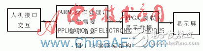
1 Scheme design and working principleThe scheme architecture of this article is shown in Figure 1, which is mainly divided into two parts: ARM operation processing and FPGA receiving display data. Its core is to replace the internal display buffer of ARM with FPGA, while increasing the processing speed of ARM, the width of ARM display data is increased from 16 The bit is increased to 32 bit, which improves the performance of industrial LCDs as a whole.
1.1 ARM operation processing
ARM operation processing structure is shown in Figure 2. The screen information is downloaded to the NAND Flash through the human-computer interaction interface and the MCU. When the display is required, the MCU reads the screen and sends the data to be displayed to the FPGA according to the requirements. In order to achieve the effect of high image quality and fast screen refreshing, NAND Flash and SDRAM adopt the design of 32 bit data width, MCU internal processing uses 32 bit mode, and the data that needs to be displayed is directly sent out 32 bit.
1.2 FPGA receives display data
The FPGA operation processing structure is shown in Figure 3. FPGA mainly completes the following tasks: generating read-write display control part according to the liquid crystal display timing; storing the received data in DDR; reading the data to be displayed from DDR, converting the data to be displayed into the LVDS signal format, and outputting and driving the liquid crystal The display.
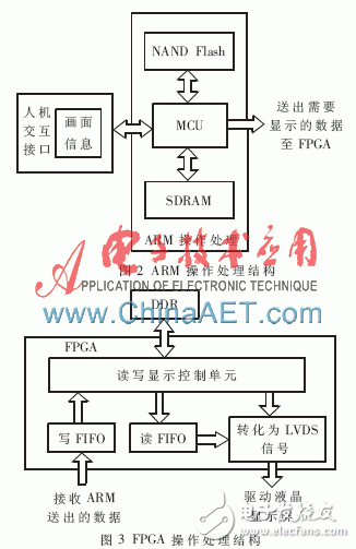
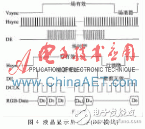
1.2.1 Design of read-write display control unit Design the read-write display control unit according to the LCD display timing. Although the timing of various LCD screens is different, the principle [2] is the same, as shown in Figure 4, including the display clock DCLK, display data RGB_data, field frequency Vs, line frequency Hs, field blanking and line blanking, as long as they meet The above conditions can drive the display. During the line blanking period, the data to be displayed in each line is read from the DDR to the read FIFO for the display of the line. After the read operation of each line is completed, the data in the write FIFO is stored in the DDR.
1.2.2 LVDS signal design
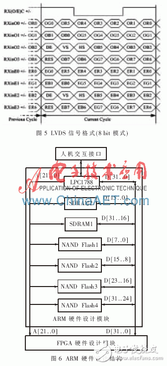
The data transmitted in the LVDS signal is arranged and displayed according to the LVDS signal format. The design of the LVDS signal is to convert the RGB888 data, DE enable signal and clock signal to be displayed into the LVDS signal format shown in FIG. 5 [3].
The hardware design is mainly divided into ARM hardware design module and FPGA hardware design module.
2.1 ARM hardware design
The ARM hardware design part is mainly composed of an ARM chip 1788, four 8-bit NAND Flash memory chips and two 16-bit SDRAMs, as shown in Figure 6. LPC1788 receives screen information through parallel port, serial port or USB interface, and stores it in NAND Flash in advance after processing; reads the screen information to be displayed from NAND Flash according to user needs, and cooperates with SDRAM operation to send the screen to be displayed to FPGA The hardware design module carries out the next operation of driving the display screen.
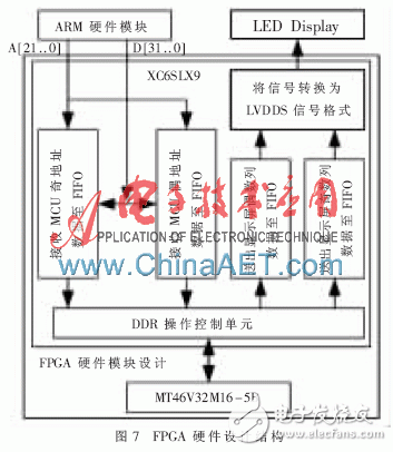
2.2 FPGA hardware module design
The FPGA hardware design module is mainly composed of a piece of Xilinx XC6SLX9 chip and a piece of Magnesium MT46V32M16-5B, as shown in Figure 7. The hardware structure that needs to be designed inside XC6SLX9 includes: receiving the data to be displayed sent by LPC1788; reading the display data from MT46V32M16-5B and converting it to the LVDS driver display.
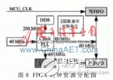
In order to facilitate processing and ensure the stability and reliability of the system, the internal clock resource allocation of the FPGA chip XC6SLX9 is shown in Figure 8. The external clock 40 MHz is input to the FPGA internal clock phase-locked loop, which is designed to output 200 MHz to MT46V32M16-5B; 80 MHz to DDR operation control unit, write FIFO read clock and read FIFO write clock; 400 MHz to LVDS signal generation At the same time of the module, 57.14 MHz is output to the read clock in the read FIFO through frequency division by 7. Among them, the write clock of write FIFO comes from MCU_CLK of LPC1788.
Fiber Optic Cables,Fiber Patch Cables,Fiber Cable Connector,Fiber Optic Line
CIXI LANGUANG PHOTOELECTRIC TECHNOLOGY CO..LTD , https://www.cxblueray.com