Design and simulation of four redundant communication boards based on CAN core
Design and simulation of four redundant communication boards based on CAN core
With the continuous development of electronic technology, computer application technology and EDA technology, the development of digital systems using FPGA has been widely used in communications, aerospace, medical electronics, industrial control and other fields. FPGA has become one of the preferred methods of hardware design today. PC / 104 is an industrial control bus specifically defined for embedded control. It is widely used for its unique stack structure and low power. As a mainstream field bus, the industrial control area network CAN (Controller Area Network) bus has strong anti-interference ability, is easy to network, and has a very broad application prospect. The unique combination of PC / 104 bus and CAN bus has further expanded the application field of CAN bus.
1 CAN core design based on FPGA
This design uses Altera's Cyclone III series FPGA EP3C25, and the development platform uses Altera's Quartus II software. The design of the CAN core is based on the SJA1000 functional structure.
The functional block diagram of CAN core is shown as in Fig. 1. The CAN bus controller IP core complies with the CANbus 2.0 standard, and its functions and register operations are compatible with SJA1000. The IP core adopts VHDL coding and adopts a fault-tolerant design, which can suppress the data bit flip of the storage device and greatly improve the reliability of the IP core. The CAN core can be implemented in FPGA or ASIC. It contains 3 main modules: register set (can_registers), bit sequential logic (can_btl), bit stream processor (can_bsp). 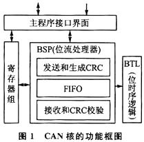
Register group (CAN Register): external microprocessors can directly access these registers by address. When sending data, the microprocessor writes the data to be sent to the send buffer, and sets the send request bit of the command register to start sending. After receiving the data, the core controller stores it in the receive buffer and informs the bit controller to remove it. At the same time, there is also a 64-byte receive FIFO in the CAN register, which can store at least 2 data frames at a time.
Bit timing logic (BTL): used to monitor the CAN bus and process the bit timing associated with the CAN bus. At the beginning of the message, when the bit sequential logic detects a transition from the recessive bit to the dominant bit on the bus, it synchronizes its internal logic to the bit stream, called hard synchronization; then In the process of receiving the message, when the transition from the recessive bit to the dominant bit is detected, it will resynchronize to the bit stream, which is called soft synchronization. Bit timing logic also determines the position of the sampling point of each bit period according to the values ​​of bus timing register 0 and bus timing register 1 to compensate for errors caused by transmission delay and phase drift; at the same time, according to the setting of bus timing register 1 The corresponding sampling mode (single sampling or 3 times) samples the data on the bus.
Bit stream processor (BSP): It is divided into 3 modules according to the functions it realizes: data receiving module, data sending module and error processing module. The data receiving module removes the bit filling from the sampled data sent from the bit timing logic and sends it to the shift register for serial-to-parallel conversion. After that, it performs a CRC check on the parallel data and sends a response signal when the message is received, indicating that the reception is correct. Finally, the signature of the received message is compared with the content of the acceptance mask register to decide whether to write the received message into the receive FIFO. The data receiving module frames the data to be sent and performs CRC calculation, and then sends it to the shift register for parallel-serial conversion, and then encodes the serial data (bit stuffing) and sends it to the bus. The error monitoring module detects system errors according to the error monitoring mechanism described in the protocol specification and sets corresponding registers to notify the device controller. According to the 12 error monitoring rules described in the protocol, the module can increase, decrease or clear the counter under appropriate circumstances. The controller determines its own fault state based on the values ​​of these two counters and the value of the error limit register: Error AcTIve, Error Passire, or Bus Off On.
2 hardware circuit design
According to the overall design of the system, because the maximum operating frequency of the existing CAN bus transceiver is 1 MHz, after increasing the CAN communication speed, the existing CAN bus transceiver cannot meet the needs, so the RS485 transceiver is used instead . Because the RS485 transceiver is a differential transmission, it cannot complete the spontaneous self-reception function of the communication card, so an external CAN Hub is required. In addition, to carry out optical fiber transmission, to complete the optical logic bus structure, an external Hub is also required. Therefore, this hardware design is divided into two parts: the design of CAN communication board and the design of CAN Hub.
(1) CAN communication board hardware circuit design
The core device of the CAN communication board is an FPGA, which simultaneously completes the "dual-light dual-electricity" communication. The structure of the hardware communication board is shown in Figure 2. 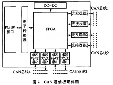
As a module of the PC / 104 system, it must be connected to the PC / 104 bus, so it must be consistent with the bus standard specified by the PC / 104 standard on the data, address, and control bus.
This design needs to carry on four redundant designs, add 4 CAN cores in the design, choose FPGA EP3C25 of Cyclone II series of Altera Company.
Because the working voltage of PC / 104 is 5 V, and the working voltage of FPGA is 3.3 V, a level shifter 74LVC245 should be added between PC / 104 and FPGA to protect the FPGA.
(2) Optical transceiver circuit
The high-speed optical transmitter of this system adopts HFBR-1414 low-power high-speed optical transmitting device, and its optical emission wavelength is 820 nm. This transmitter can be used with the following 4 optical fibers: 50/125 μm, 62.5 / 125 μm, 100/140 μm, 200 μm (HCS). HFBR-1414 uses a double-lens optical system with high light emission efficiency. When the drive current is 60 mA, -15 dBm optical power can be obtained on 50/125 μm fiber. The optical receiver uses HFBR-2412, which integrates a photodiode, DC circuit and open collector Schottky transistor. The HFBR-2412 optical receiver can be used with the optical transmitter HFBR-1414 and 50/125 μm, 62.5 / 125 μm, 100/140 μm, and 200 μm (HCS) optical fibers, with a maximum communication rate of 5 MB. Thanks to the open collector circuit, this receiver is compatible with TTL and CMOS levels. The communication distance of this circuit can be up to 1.7 km.
In order to improve the comprehensive performance of CAN communication board, such as anti-vibration and anti-interference, a double-sided wiring design is adopted. The size of the communication board is strictly in accordance with the requirements of the PC / 104 board.
(3) Redundancy design and CAN Hub design
The communication board is designed with 4 channels of redundancy. When working, only 1 channel of CAN channel is used to work. The high-level chip selection is used to select the working channel. The chip selection module is designed inside the FPGA.
(4) Design of GAN Hub
Because this system adopts the "double optical double electricity" four redundant circuit design, in order to improve the communication speed, the 485 transceiver is used instead of the standard CAN transceiver. Only the "point-to-point" transmission, the 485 transceiver is differential transmission, and it can not form a bus structure in form. Therefore, the introduction of CAN Hub to process the signal, logically achieve a bus-type structure.
3 software design
The normal work of the CAN communication board is inseparable from the powerful software support. The core of the control part in this system uses the PC / 104 embedded computer system. The PC / 104 embedded computer has powerful functions comparable to that of the PC. The development and design of the CAN communication board software part is completed on the PC / 104 computer and is designed in C language. The C language is versatile, efficient and real-time, and can meet the real-time requirements of the instrument. In the design process, a modular and structured design method is adopted, and the software is divided into several modules according to functions. These modules have both certain independence and certain connections. The preparation requirements of each module are relatively independent in order to inspect, debug, modify and maintain each module. The program of this framework mode can ensure good versatility, maintainability, scalability, portability, interchangeability and independence.
Because the internal structure of the CAN core is the same as that of the SJA1000, it is as simple and convenient to write as when facing the SJA1000 during development. This design uses interrupt processing to process tasks. After the interruption arrives, it can be dealt with accordingly.
The communication board initialization process is shown in Figure 3. 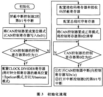
The data sending process is shown in Figure 4, and the data receiving process is shown in Figure 5. 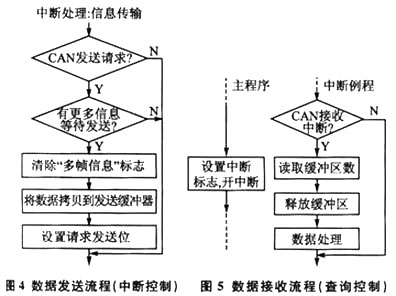
4 System Simulation
Use Modelsim for simulation.
The system's test platform (TestBench) instantiates the module can4core and a CAN core cantop, and simulates the communication between them.
This simulation is carried out in full accordance with the normal working process of the CAN core. The simulation process is as follows:
â‘ Initialize the settings. First, set the time register and data format. Set up the system design module and CAN core through the platform.
â‘¡ Simultaneous testing. Including hard synchronization test and resynchronization test. After a hard synchronization, the internal bit time restarts with the synchronization segment. Hard synchronization causes the edge that caused the hard synchronization to lie within the restarted bit time synchronization segment.
â‘¢ Empty FIFO test (test_empty_fifo_ext). This test is to receive 2 data frames, then read the receive buffer, then clear the buffer, then read the buffer, repeatedly empty and read, to see if the data in the FIFO is completely cleared.
â‘£Full FIFO test (test_full_fifo_ext). First clear the register, then fill the FIFO and read the information by continuously receiving data frames to detect whether it can work normally.
⑤ Bus idle test (bus-off-test). The bus is kept busy by sending data continuously, causing the bus to generate errors, testing whether the interrupt register can detect the error, and whether the CAN core can continue to work normally after the error is cleared.
â‘¥Basic CAN mode sending frame detection. Test whether the CAN core can send frames normally.
⑦ Register test. By continuously reading and writing registers, it is checked whether the CAN core register works normally.
⑧Data transmission on the bus. An important point in the simulation process is whether the data information can be normally transmitted on the bus.
After simulation, we can see that the CAN communication board has broken through the speed limitation of SJA1000, the transmission speed can reach 2 MHz, the effective transmission rate has been greatly improved, and the working performance is good.
Conclusion
The CAN bus communication board designed in this paper completes the communication conversion between PC / 104 and CAN bus, and changes the traditional design method of using CAN controller plus external controller. Based on the design of CAN core, all digital signals in the communication board The processing part is implemented inside the FPGA, which greatly improves the communication speed. Whether in the transmission rate or in anti-jamming, seismic resistance, etc., the comprehensive performance of the CAN core application has been greatly improved.
Tinned Copper Clad Copper TCCC
Corrosion-Resistant Copper-Clad Tinned Wire,Copper-Clad Copper Tinned Wire Production,Copper-Clad Copper Tinned Wire Processing,Copper-Clad Tinned Wire
changzhou yuzisenhan electronic co.,ltd , https://www.ccs-yzsh.com