Detailed analysis of the reverse steps of the PCB schematic and details to be noted
PCB copy board, also known in the industry as board copy board, board cloning, board copying, PCB cloning, PCB reverse design or PCB reverse development. That is, under the premise that there are physical objects and circuit boards in the electronic product, the reverse analysis technology is used to reversely analyze the circuit board, and the original product PCB file, bill of materials (BOM) file, schematic file and other technical documents and PCB silk screen production files are restored 1:1, and then these technical documents and production files are used for PCB board, component soldering, flying probe testing, circuit board debugging, and complete copying of the original circuit board template.
For PCB copy board, many people don't understand, in the end what is PCB copy board, some people even think that PCB copy board is a cottage. In the understanding of everyone, the cottage is the meaning of imitation, but the PCB copy board is definitely not an imitation. The purpose of PCB copy board is to learn the latest electronic circuit design technology in foreign countries, and then absorb the excellent design scheme, and then use it to develop better design. The product. 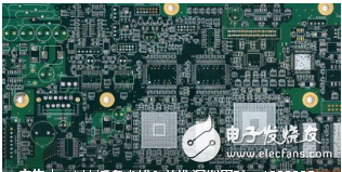
With the continuous development and deepening of the copy board industry, today's PCB copy board concept has been extended to a wider scope, no longer limited to simple board copying and cloning, but also involves secondary development of products and new products. Research and development. For example, through the understanding and discussion of the analysis of existing product technical documents, design ideas, structural features, process technology, etc., it can provide feasibility analysis and competitive reference for R&D and design of new products, and assist R&D and design units to follow up in time. Technology development trends, timely adjustment and improvement of product design, research and development of new products with the most competitive market.
The process of PCB copying can realize the rapid update, upgrade and secondary development of various types of electronic products through the extraction and partial modification of technical data files. According to the document map and schematic drawing extracted by the copy board, professional designers can also according to the customer's Willing to optimize the design and modification of the PCB, and also be able to add new functions or redesign the functional features on the basis of this, so that the products with new functions will appear at the fastest speed and a new attitude, not only have With its own intellectual property rights, it has also won the first opportunity in the market, bringing double benefits to customers.
Whether used to analyze board principles and product operating characteristics in reverse studies, or to be reused as the basis and basis for PCB design in forward design, PCB schematics have a special role. Then, according to the document map or the real thing, how to reverse the PCB schematic diagram, what is the reverse push process? What are the details of this attention?
First, the reverse step: 1 record PCB related details to get a PCB, first record the model, parameters, and position of all components on the paper, especially the direction of the diode, the three-stage tube, the direction of the IC gap. It is best to take a photo of two component locations with a digital camera. A lot of pcb boards are getting higher and higher. The above diodes are not noticed at all. 2 The scanned image removes all devices and removes the tin from the PAD holes. Clean the PCB with alcohol and put it into the scanner. When scanning, the scanner needs to slightly raise some scanned pixels to get a clearer image. Then polish the top and bottom layers slightly with water gauze, polish it to the copper film, put it into the scanner, start PHOTOSHOP, and scan the two layers in color. Note that the PCB must be placed horizontally and vertically in the scanner, otherwise the scanned image will not be used. 3Adjust the corrected image to adjust the contrast and brightness of the canvas so that the part with the copper film and the part without the copper film are strongly contrasted. Then turn the secondary image to black and white to check whether the line is clear. If it is not clear, repeat this step. If it is clear, save the picture as black and white BMP format files TOP BMP and BOT BMP. If you find any problems with the graphics, you can use PHOTOSHOP to fix and correct them. 4 Verify the positional coincidence degree of PAD and VIA Convert the two BMP format files into PROTEL format files respectively, and transfer them into two layers in PROTEL. For example, the positions of PAD and VIA over two layers are basically coincident, indicating the first few steps. Do a good job, repeat the third step if there is a deviation. Therefore, pcb copy board is a very patient work, because a small problem will affect the quality and the degree of matching after copying. 5 draw the layer to convert the TOP layer BMP into TOP PCB, pay attention to the SILK layer, which is the yellow layer, then you draw the line in the TOP layer, and place the device according to the drawing in the second step. Remove the SILK layer after painting. Repeat until you have drawn all the layers. 6TOP PCB and BOT PCB mapping In the PROTEL, the TOP PCB and BOT PCB are transferred, and it is OK to combine them into one figure. 7 laser printing TOP LAYER, BOTTOM LAYER prints TOP LAYER, BOTTOM LAYER to transparent film (1:1 ratio) with laser printer, put the film on the PCB, compare whether it is wrong, if it is correct, You are done. 8 test test copy board electronic technical performance is not the same as the original board. If it is the same, it is really done. Second, pay attention to details1. Reasonable division of functional areas
When the reverse design of the schematic of a good PCB board, the reasonable division of functional areas can help engineers reduce unnecessary troubles and improve the efficiency of drawing. In general, components with the same function on a PCB will be arranged in a centralized manner, and the functional division area can have a convenient and accurate basis when deducing the schematic.
However, the division of this functional area is not arbitrary. It requires engineers to have a certain understanding of electronic circuit related knowledge. First, find out the core components in a functional unit, and then find out the other components of the same functional unit according to the connection of the traces to form a functional partition. The formation of functional partitions is the basis for schematic drawing. In addition, in the process, don't forget to use the component serial numbers on the board, they can help you to partition the function faster.
2. Find the reference piece
This reference piece can also be said to be the main component PCB network city at the beginning of the schematic drawing. After determining the reference part, drawing according to the pins of these reference parts can ensure the accuracy of the schematic diagram to a greater extent. Sex.
For the engineer, the determination of the reference part is not a very complicated matter. In general, the components that play a major role in the circuit can be selected as the reference parts. They are generally bulky and have many pins, which are convenient for drawing. Such as integrated circuits, transformers, transistors, etc., can be used as a suitable reference.
3. Correctly distinguish the lines and draw the wiring reasonably
For the distinction between ground, power, and signal lines, engineers also need to have relevant power knowledge, circuit connection knowledge, PCB wiring knowledge, and so on. The distinction between these lines can be analyzed from the connection of components, the width of the copper foil of the circuit, and the characteristics of the electronic product itself.
In the wiring drawing, in order to avoid the intersection and interweaving of the line, the grounding symbol can be used in a large amount on the grounding wire. Various lines can be clearly distinguished by using different lines of different colors, and special symbols can be used for various components, and even The unit circuits are drawn separately and finally combined.
4. Master the basic framework and draw on similar schematics
For the framework of some basic electronic circuits and the principle drawing method, engineers need to master, not only to directly draw the basic composition of some simple and classic unit circuits, but also to form the overall framework of electronic circuits.
On the other hand, don't neglect that the same type of electronic products have certain similarity in the schematic diagram of PCB network city. Engineers can make full use of similar circuit diagrams to carry out the reverse of new product schematic diagrams based on the accumulation of experience.
5. Check and optimize
After the schematic drawing is completed, it is necessary to pass the test and check link to conclude the reverse design of the PCB schematic. The nominal value of the component sensitive to the PCB distribution parameters needs to be checked and optimized. According to the PCB file diagram, the schematic diagram is compared and analyzed to ensure that the schematic diagram and the file diagram are completely consistent.
Interface Drivers Receivers Transceivers
Shenzhen Kaixuanye Technology Co., Ltd. , https://www.iconlinekxys.com