FPGA-based Vivado power estimation and optimization
Resources, speed and power consumption are three key factors in FPGA design. With the development of the process level and the improvement of system performance, low power consumption has become one of the goals of some products. Power consumption has also attracted the attention of more and more system engineers and FPGA engineers. Xilinx's next-generation development tool, Vivado, has a comprehensive methodology and strategy for power consumption. This article will show you how to use Vivado for power analysis and optimization.

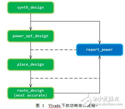
Under Vivado, any DCP file generated from the integrated design to the post-layout design can be used for power estimation, as shown in Figure 1. After opening the integrated design or the layout and layout design, you can select Report Power in the graphical interface mode, or you can use the Tcl command report_power to obtain the power estimation result. Among them, the use of the layout and layout design can obtain more accurate power estimation results.
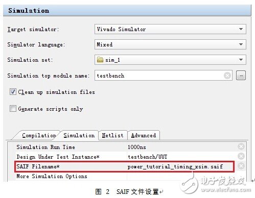
Under Vivado, there are two power estimation modes. One is vector mode, which needs to provide SAIF (Switching AcTIvity Interchange Format) or VCD file; one is non-vector mode, only need to provide simple parameters, but the estimation result is not accurate enough. The SAIF file is generated by simulation, so it needs to be set in SimulaTIon SetTIngs, as shown in Figure 2. The simulation here can only be the integrated function/timing simulation or the post-placement function/timing simulation, which is determined by the flow of Figure 1. Xilinx recommends selecting the SAIF file in vector mode because it is estimated to be faster than VCD.
After selecting Report Power, the interface shown in Figure 3 pops up, and the corresponding parameters are filled in. If it is vector mode, select the corresponding SAIF file in the Switching window, as shown in Figure 4. You can see that Report Power is able to generate the files needed for XPE power estimation. The results of the power estimation are shown in Figure 5. It can be seen that the convergence level of the vector mode result is high and the non-vector mode is low. The reason for this is that the SAIF file provides the internal signal and the flip rate of the external I/O port signal, as shown in I/O AcTIvity and Internal Activity in Figure 6.
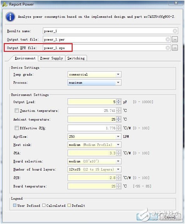
Figure 3 Report Power interface
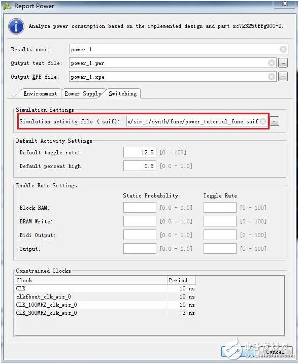
Figure 4 SAIF file interface in Report Power
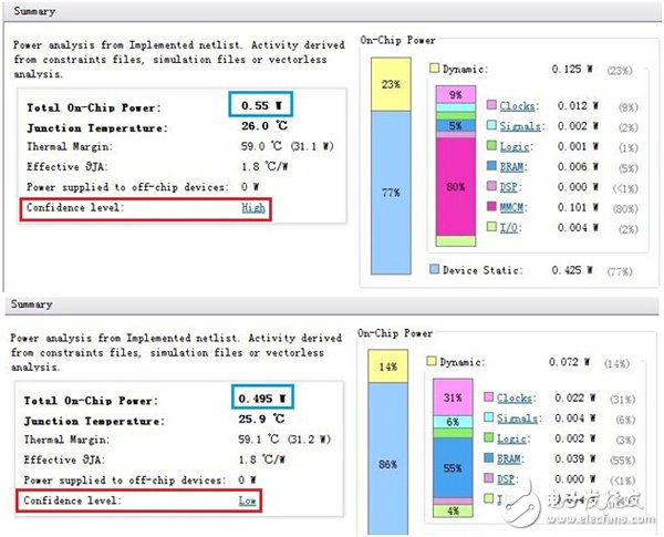
Figure 5 power estimation results

Figure 6 Reasons for confidence level high and low
Power optimizationIn the Implementation phase, there is a process specifically optimized for power consumption, as shown in Figure 7. There is power_opt_design before the layout, and power_opt_design after the layout. In contrast, power_opt_design prior to layout is more thorough and comprehensive in optimizing power consumption.
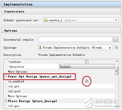
Figure 7 Flow chart for power optimization
Select is_enabled in Figure 7, and run implementation. After opening the layout design, select Tool>Report>Report Power Optimization from the menu, or use the Tcl command report_power_opt to view the power_opt_design optimization report for power consumption. 8 is shown. It can be seen that Vivado achieves the goal of reducing power consumption by adding an enable signal to the BRAM (TOOL GATED in the figure) to control the flip rate of the signal.

Figure 8 Power Optimization Report
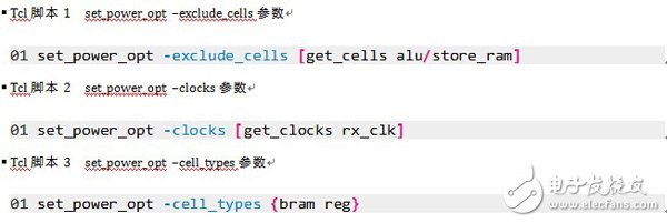
The goal of power optimization is to minimize FPGA power while minimizing its impact on timing. However, sometimes the power consumption is optimized (running power_opt_design). The timing is worse or even unable to converge. In this case, the power-optimized object can be controlled by the Tcl command set_power_opt. For example, the store_ram in the alu module is not optimized, and can be implemented by Tcl script 1. If only a certain clock domain is optimized, it can be implemented by Tcl script 2; if only a certain type of cell is optimized, it can be implemented by Tcl script 3. .
In summary, in order to obtain a more accurate estimation of power consumption, the SAIF file should be provided as much as possible, and at the same time, all the clocks in the design should be reasonably constrained. In addition, a larger control signal for the fanout should be given. Its flip rate. Power optimization should be considered at the beginning of the design. The RTL code style should be followed in the design. For example, try to avoid asynchronous reset or set of flip-flops and BRAM, and select power_opt_design before layout and power_opt_design after layout. The optimization object is managed by set_power_opt according to the influence of power optimization on the design timing.
Stainless Steel Non-Magnetic Wire
Stainless Steel Non-Magnetic Wire,Cable Wire Railing Stainless Steel,309L Flux Core Wire,Marine Grade Non-Magnetic Stainless Steel Wire
ShenZhen Haofa Metal Precision Parts Technology Co., Ltd. , https://www.haofametal.com