FPGA Implementation of Wideband IF Digital Receiver
Pick    To: This paper proposes an implementation method of wideband IF digital receiver based on FPGA .
introduction
In modern communication systems, various all-digital modulation and demodulation schemes have been proposed, and the research of all-digital receivers is the key. The quadrature demodulation technology can realize the extraction of signal phase and amplitude information. Therefore, it is more and more widely used.
Compared with other demodulation methods, the QPSK modulation method has good anti-noise performance, less power spectrum segment occupation, and high data transmission rate, which is a better modulation method. For wideband, high carrier frequency QPSK modulated signals, if the clock is sampled with more than twice the highest frequency of the signal, the existing devices cannot meet the requirements at all. Therefore, undersampling technology must be used to reduce the performance of the system for ADC devices and signal processing devices. Claim.
Nowadays, large-scale integrated circuit design has been developed to integrate a complex system on a chip, so a single-module, single-chip receiver is not only achievable, but also an inevitable trend. Using the software to realize the receiver demodulation function and using the high-speed FPGA chip, the entire receiver demodulation part can be realized by a single chip; by modifying the software, the function of the receiver can be changed, and since it is a module in software and hardware, It is easy to expand functions and connect with other systems, which is also in line with the idea of ​​software radio. Based on the above reasons, a wideband IF digital receiver system implemented by a single chip FPGA is proposed .

Figure 1 Â Â IF digital receiver
Â

Figure 2 Â Â NCO structure diagram

Figure 3 Â Â Demodulator software implementation
system structure
The receiver realizes demodulation of a QPSK modulated signal with a carrier frequency of 70 MHz , a data rate of 9.856 Mbps , and a maximum carrier frequency offset of ± 80 kHz . The received modulated signal passes through the AGC and the bandpass filter, and is sampled by the high-speed ADC IF, and the digital signal is sent to the FPGA to implement the demodulation function ( see Figure 1) .
Since the received signal is a high carrier frequency bandpass signal, undersampling techniques must be used. For this system, the signal carrier frequency is 70MHz and the bandwidth is about 10MHz .
Fh=n · B+k · B
Where B is the bandwidth , here take 10MHz, n=7, k=0.5 According to the sampling theorem, the lowest sampling frequency is:
Fs=2B(1+k/n)
Approximately equal to 21.4MHz . The selection of the sampling frequency should consider two factors: First, the sampling theorem of the band-pass signal should be satisfied, and the spectrum cannot be aliased after sampling; second, the data rate after sampling should meet the requirements of the latter processing. For the sampling frequency of the system selected 40MHz , the sampled signal spectrum will be mirrored to a frequency band of 10MHz with a center bandwidth of 10MHz .
After the A/D conversion, the digital signal is directly into the FPGA to perform demodulation, and the modulated data is extracted. Due to the use of full digital demodulation, the characteristics of the I and Q digital mixers and filters are identical, which avoids the I and Q channels caused by the unsatisfactory consistency and stability of the analog device during analog demodulation. A phenomenon in which the amplitude is unbalanced and the phase quadrature error is large. For a receiver using coherent demodulation, since the received modulated signal usually has Doppler shift and carrier frequency difference, the demodulation performance mainly depends on the accuracy of carrier recovery and clock extraction.
The carrier recovery circuit uses a digital COSTAS loop, which combines carrier extraction and demodulation to complete the demodulation function while extracting the carrier. The loop has a rectangular phase discrimination characteristic with a small static phase difference and a large locking bandwidth. Meanwhile, the phase discrimination characteristic has a quadruple phase ambiguity, so an absolute / relative code conversion circuit must be added during modulation . A relative / absolute code conversion circuit is added to the demodulation to overcome the phase ambiguity. The core of the carrier recovery circuit is the generation of the local oscillator source. In the digital circuit, the digital oscillator source (NCO) is used to generate the local carrier. The NCO ( see Figure 2) has a fast frequency agility, a relatively wide bandwidth, and a high frequency resolution. It can output two orthogonal carriers that are completely orthogonal.
The output frequency of the NCO is:
Fnco=DF · fclk/2 π =FCW · fclk/2a
Where FCW is the frequency control word, a is the frequency control word length, and fclk is the clock frequency.
The clock extraction ( bit synchronization ) adopts a lead - lag digital phase-locked loop circuit, and the input phase reference is phase-compared with the phase pulse divided by the local reference clock n times to generate a lead or lag pulse, and the symbol synchronization is adjusted under the action of the control circuit. The phase of the pulse. The principle of adjustment is that when the reference phase pulse leads the input phase reference, the phase comparator outputs a lead pulse, triggering the deduction gate to subtract one pulse, and the phase of the reference phase pulse is pushed back by 1/n period; conversely, when the reference phase pulse lags behind When the phase reference is input, the phase comparator output hysteresis pulse triggers the add gate to add a pulse, and the phase of the reference phase pulse is advanced by 1/n cycle. After the phase is adjusted repeatedly, the symbol synchronization is realized, and a bit synchronization clock is generated.
After carrier recovery and clock synchronization are completed, symbol discrimination, relative code / absolute code conversion, and parallel / serial conversion are performed, and finally, demodulated data is output.
Software receiver and hardware implementation
In modern electronic design, in order to shorten the design cycle, Electronic Design Automation (EDA) has gradually become the key to the success of project design. Quartus  II is an FPGA development platform provided by Altera Corporation . It integrates all the tools required for FPGA development such as editing, simulation, synthesis, and chip programming. Together with other system-level simulation software, it can greatly shorten the system design cycle. The FPGA chip uses Altera 's EP1S10 series, which has rich internal resources and complete external interfaces.
The main resources of the integrated chip are as shown in Table 1 .
In the software implementation process, the most important thing is to correctly and effectively implement high-speed, complex combinational logic and sequential logic circuits, and implement system functions with an integrated hardware description language program. Since the demodulation part is all completed in the FPGA , the whole system only needs one FPGA chip and corresponding configuration chip and A/D converter, analog filter, RF processing circuit plus power supply circuit and signal output interface, the hardware structure is very simple.
System simulation and measured results
Figure 4 shows the simulation results of the system when the carrier frequency difference is +20KHz . Figure 5 shows the demodulation results of the I and Q channels displayed on the oscilloscope when the system hardware is actually measured .
Conclusion
After the actual hardware test, each functional module works normally, and the receiver fully meets the system design requirements; and the system structure is simple, the power consumption is low, and the debugging is convenient. With the continuous development of large-scale integrated circuit design technology, the generation of high-speed digital signal processors and the application of efficient EDA tools, modular integration of complex systems will become easier. â–
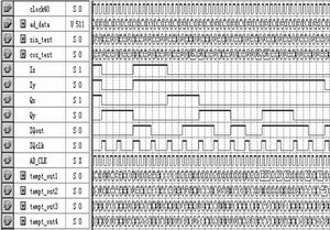
Figure 4 Â Â System simulation result
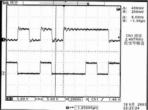
Figure 5 Â Â I , Q demodulation measured results
Fc To Lc Adapter,Fiber Cable To Ethernet Converter,Fiber Optic Adapter Kit,Fiber To Ethernet Converter
Ningbo Fengwei Communication Technology Co., Ltd , https://www.fengweifiberoptic.com