Frequency follow-up based on SERDES clock
Preface In many wireless or wired system applications, the receiving end of the device needs to follow the frequency of the transmitting end of the link. The usual implementation is to bring the recovery clock of the SERDES to the outside of the chip, then filter the jitter through a cleanup PLL, and then regenerate the following clock with low phase jitter, and then use this clock as the reference clock for the SERDES. The typical scene is as follows:
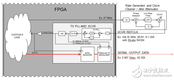
Figure 1 Traditional frequency following scheme
However, such a solution is obviously not suitable for applications that require a frequency following interface, such as a POS interface. The PI (Phase Interpolator) function of the XILINX 7 Series SERDES transmitting side provides a perfect solution for this type of application scenario.
XILINX SERDES send side PI function introductionThe structure of the transmission direction of the XILINX 7 Series SERDES is as follows:
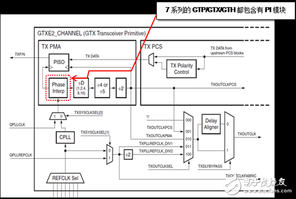
Figure 2 7 series SERDES transmission direction structure diagram
This PI module can interpolate the transmit serial clock of the SERDES as required to adjust the frequency. With this function, if we can adjust the transmit serial clock of the SERDES based on the offset of the transmit side clock and the receive side's recovered clock, then the frequency following function we need will be implemented. The basic implementation block diagram is as follows:
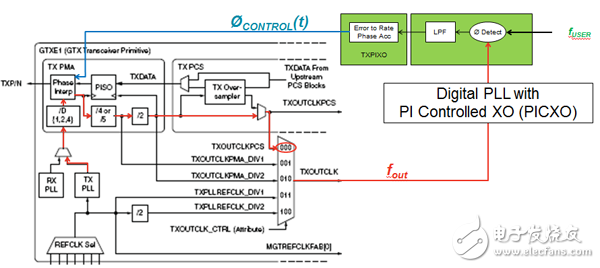
Figure 3 Basic block diagram of the frequency following scheme of the XILINX 7 series SERDES
PICXO IP IntroductionFor the system architecture shown in Figure 2, XILINX provides a complete IP solution. See XAPP589() for details. The block diagram of the PICXO IP is as follows:
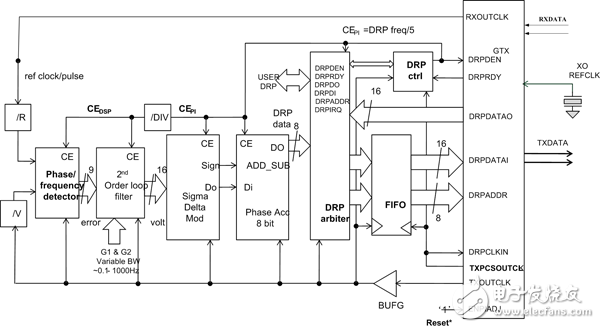
Figure 4 PICXO block diagram
The key to PICXO IP is the DPLL functionality it provides. This IP provides a rich configuration interface that allows users to generate the loop filtering bandwidth they need. The Hold function is also provided to meet certain scene applications that require the Holdover function.
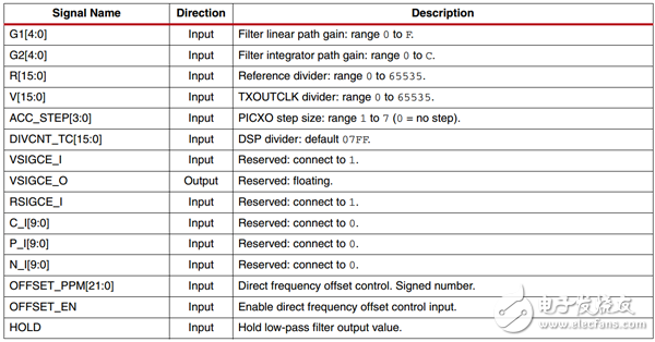
Figure 5 PICXO configuration interface
By adjusting the parameters of the DPLL (G1, G2, R, V, ACC_STEP, DIVCNT_TC), digital low-pass filters of various bandwidths can be generated. The figure below shows the jitter transfer function in various configurations.
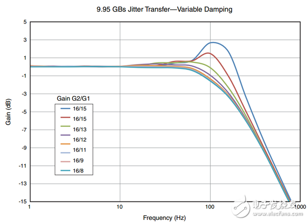
Figure 6 PICXO jitter transfer function
Performance test resultThe PI function provided by the XILINX 7 series SERDES can meet most of the frequency following applications in current communication applications. Take the common POS interface and OTUe2 interface test as examples, which can meet the requirements. The following figure shows the test results of OC-192:
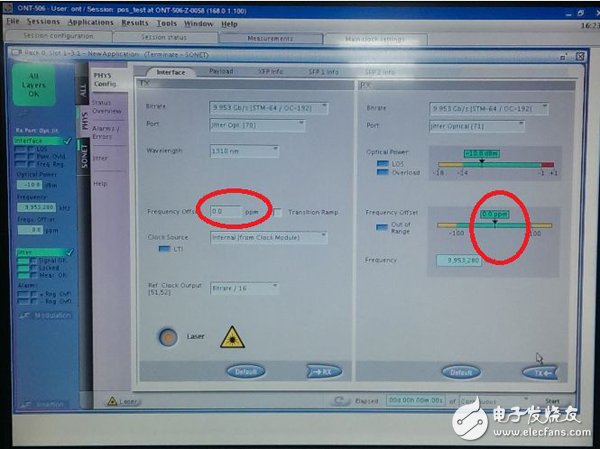
Figure 7 PI function demonstration Figure 1
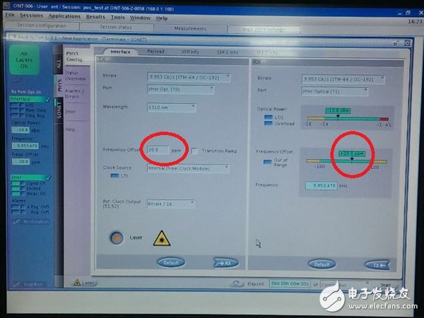
Figure 8 PI function demonstration Figure 2
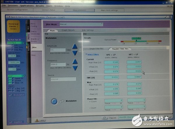
Figure 9 Transmit jitter test in OC-192 application
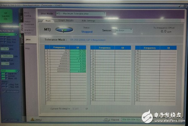
Figure 10 Receive jitter tolerance test for OC-192 applications
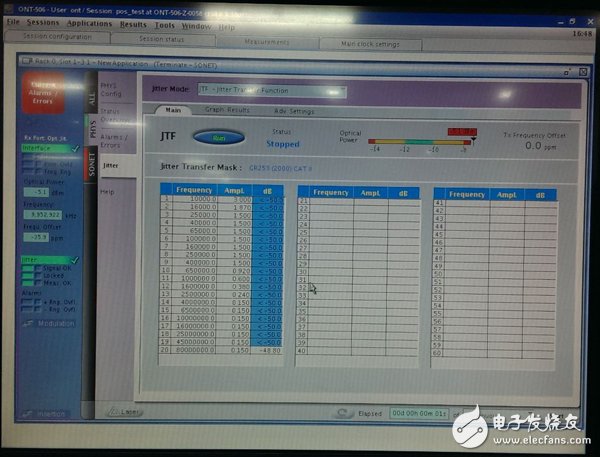
Figure 11 Receive jitter transfer function test in OC-192 application
postscriptThanks to the excellent performance of XILINX's QPLL and PI, it provides a very competitive solution when you need to do frequency following. Cost, board area and power consumption can be balanced. It has been widely used by large equipment manufacturers.
Sfx Power Supply,Sfx 250W Power Supply,Sfx Pc 150W Power Supply,Psu 150W 200W Power Supply
Boluo Xurong Electronics Co., Ltd. , https://www.greenleaf-pc.com