Implementation of Channel Estimation for a MIMO-OFDM Video Transmission System
Channel estimation is a key technology in OFDM. Its purpose is to give the channel parameters needed for channel equalization, signal detection, channel quality measurement and soft decoding at the receiving end. The performance is directly related to the entire OFDM communication system. Rate performance [1] [2].
The channel estimation method based on reference signal (RS) mainly includes LS algorithm and MMSE algorithm: LS algorithm is simple and suitable for general wireless environment; MMSE algorithm is highly reliable, but too complicated [3] [4]. The channel estimation on the OFDM system combining MIMO technology should consider separating the pilots that receive multiple transmit antennas from each receiving antenna, and coordinate the processing of receiving data from multiple receiving antennas [5]. At present, there are few design schemes for channel estimation in MIMO-OFDM system on FPGA. In some traditional schemes [5]-[7], each channel needs to set a channel estimator to estimate the pilot position channel frequency response, and interpolate. Estimated by a complex multiplier, this will consume a lot of hardware resources. Based on the MIMO-OFDM system in [8], this paper designs and implements channel estimation on the ML605 development board. According to the system application environment, considering the resource consumption and complexity, the LS estimation algorithm and the linear interpolation algorithm are used for modular design, which has good scalability. The LS estimation module is simplified based on the traditional channel estimation scheme, and the interpolation coefficient calculation of the interpolation module is optimized to reduce the consumption of the FPGA operation unit and the storage unit. After testing, the video signal is clear and stable after the program is added to the video transmission system.
Figure 1 shows a two-layer physical layer receive link model for real-time video transmission. After the receiver signal is demodulated by OFDM, the user data signal and the reference signal are separated. The channel estimation module multiplies the received reference signal by the conjugate of the locally stored reference signal to obtain a channel parameter [9]. According to the MIMO diversity space-frequency decoding formula, the user data signal and the channel parameters are collated and output to the MIMO decoding module. Processing to reduce wireless channel interference. The system global clock frequency is 100 MHz, the system bandwidth is 10 MHz, the number of subcarriers is 600, and MIMO uses 2T & TImes; 2R antenna matrix.
3. Overall design of the channel estimation moduleThe channel estimation module designed in this paper is first modeled on the Xlinx ISE using the VHDL language and added to the receiving chain.
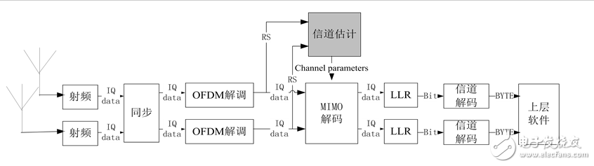
Figure 1. Architecture of receiver of video transmission system
Figure 1. Video transmission system receive link model
The simulation test is performed on the road; then the physical link is mounted as a hardware peripheral to the system on the Xlinx XPS, and the Microblaze IP core is configured; finally, the receiver and the sender are downloaded to the two ML605 development boards respectively, and are sent. The camera and the video server are terminated, and the receiving end is decoded by the decoder, and the video image captured by the camera can be seen on the display.
The channel estimation module adopts a two-layer link structure to process the received data of the two receiving antennas. The top-level module consists of four modules: LS estimation module, interpolation module, data processing module and output module, as shown in Figure 2.
In FIG. 2, RS00 and RS10 respectively represent reference signals transmitted by two transmitting antennas received by the receiving antenna 0, and RS01 and RS11 respectively represent reference signals transmitted by the two transmitting antennas received by the receiving antenna 1. After receiving the reference signal (RS), the LS estimation module estimates the channel parameter hls of the location where the RS is located, and outputs the channel parameter hls to the interpolation module; the interpolation module uses the received pilot position channel parameter according to the pilot pattern. Frequency domain and time domain interpolation calculate the channel parameter h of the user data location and store it in the RAM; the data processing module receives the user data, and sorts the data into a format required by the MIMO decoding module, and outputs the format to the output module; the output module utilizes from the OFDM The user data address received by the demodulation module extracts channel parameters of four channels (two transmit antennas to two receive antennas) of the corresponding user data position from the RAM, and outputs the user data together with the channel parameters.
In order to facilitate the optimization and upgrade of the physical link in the future, each function adopts a modular design, and the external interface of the module adopts the AXI-Stream interface uniformly, and the modules are connected by a FIFO with an AXI-Stream format interface, as shown in FIG. .
In the AXI-Stream protocol, when the rising edge of the clock arrives, the data transmission is completed when both the READY and VALID handshake signals of the receiving end or the transmitting end are "1" at the same time. When the READY signal of the FIFO output is "1", it indicates that the FIFO is not full; when the FIFO output VALID signal is "1", it indicates that there is valid data in the FIFO.
The video transmission system adopts the frame structure and pilot pattern specified by the LTE downlink [10], as shown in FIG. The white space in the pilot pattern represents resource particles (RE) carrying user data and control information, the black grid represents the RE carrying the pilot data, and the grid represents the blank RE that does not carry any information.
3.1. LS Estimation Module
The LS estimation module mainly estimates the channel parameters of the RS position by using the LS algorithm. ![]() . Let the received RS be
. Let the received RS be ![]() , the locally stored RS is
, the locally stored RS is ![]() . According to the LS algorithm:
. According to the LS algorithm:
![]() (1)
(1)
due to ![]() versus
versus ![]() All are plural,
All are plural, ![]() ,
, ![]() , brought into (1) to get:
, brought into (1) to get:
![]() (2)
(2)
According to equation (2), the LS estimator is designed using binary tree pipeline technology. The binary tree pipeline structure can fully exploit the advantages of the FPGA parallel pipeline, improve system computation efficiency, and reduce register consumption. In the pipeline design, you first need to choose the appropriate number of pipeline stages to reduce the processing delay. For example, for an algorithm in which N data is involved in processing and a result of seven multiplications or addition operations is required, the pipeline stage should be set to ![]() . Second, each stage of the pipeline can not take too much calculation, otherwise it will reduce the overall pipeline processing speed. In this paper, the design of the LS estimator uses a three-stage pipeline. Each stage of the pipeline assumes one operation task and delays one clock cycle, as shown in Figure 5.
. Second, each stage of the pipeline can not take too much calculation, otherwise it will reduce the overall pipeline processing speed. In this paper, the design of the LS estimator uses a three-stage pipeline. Each stage of the pipeline assumes one operation task and delays one clock cycle, as shown in Figure 5.
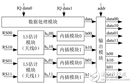
Figure 2. Architecture of channel esTImaTIon module
Figure 2. Top-level structure of the channel estimation module
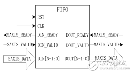
Figure 3. Architecture of AXI-Stream interface
Figure 3. AXI-Stream protocol interface structure
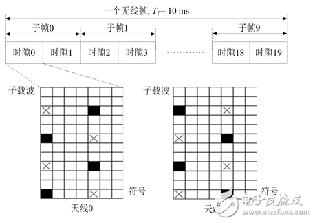
Figure 4. The frame structure and the double-antenna pilot pattern of the system
Figure 4. System frame structure and dual antenna pilot pattern
The local RS is generated by Matlab and stored in the ROM. The state machine controls the ROM address and outputs the corresponding RS. In the traditional channel estimation scheme, each receiving antenna requires two LS estimators for RS position channel parameter estimation [5] [6]. Taking the RS received by antenna 0 as an example, RS00 and RS01 respectively require an LS estimator and a ROM storing the local RS for parameter estimation. Since antenna 0 and antenna 1 transmit the same RS, in this scheme, RS00 and RS01 are combined, and the state machine control is alternately input to an LS estimator to reduce the use of resources such as the arithmetic unit and the ROM.
3.2. Interpolation module
The interpolation module performs linear interpolation based on the pilot pattern. First, the frequency domain interpolation is performed, and the pilot pattern transmitted by the antenna 0 is taken as an example. The frequency domain interpolation formula is as shown in equation (3).
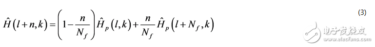
among them ![]() Indicates the frequency direction RS interval,
Indicates the frequency direction RS interval, ![]() Representation frequency
Representation frequency ![]() ,time
,time ![]() Channel response at location. The channel parameters between the RS positions on the OFDM symbol (symbol 0 and symbol 4, taking symbol 0 as an example) on which the RS is located are estimated by hls obtained from the estimation module, and stored in the corresponding FIFO. There are 100 RSs in each symbol, so the loop is 99 times. After the loop, the subcarrier channel parameters at the edge are directly assigned to the channel parameters of the nearest RS location. The process is shown in Figure 6.
Channel response at location. The channel parameters between the RS positions on the OFDM symbol (symbol 0 and symbol 4, taking symbol 0 as an example) on which the RS is located are estimated by hls obtained from the estimation module, and stored in the corresponding FIFO. There are 100 RSs in each symbol, so the loop is 99 times. After the loop, the subcarrier channel parameters at the edge are directly assigned to the channel parameters of the nearest RS location. The process is shown in Figure 6.
Then perform time domain linear interpolation, and the time domain interpolation formula is as shown in equation (4):
among them ![]() Indicates the time direction pilot interval,
Indicates the time direction pilot interval, ![]() Representation frequency
Representation frequency ![]() ,time
,time ![]() Channel response at location. Channel parameters of symbol 0 and symbol 4 obtained by frequency domain interpolation in fifo are used to estimate channel parameters of all subcarriers on other symbols, and map them to corresponding addresses in corresponding symbol RAM, so that the output module can use the received data. The address reads the channel parameters of the corresponding location. Since the number of subcarriers configured in the system is 600, the cycle is set 600 times. The channel parameters of each symbol of symbol 0 and symbol 4 in the time domain interpolation need to be used twice, so after the first reception and interpolation calculation, the symbol channel parameters will be stored in the temporary fifo (temp) for the next time. Round cycle interpolation is used. The process is shown in Figure 7.
Channel response at location. Channel parameters of symbol 0 and symbol 4 obtained by frequency domain interpolation in fifo are used to estimate channel parameters of all subcarriers on other symbols, and map them to corresponding addresses in corresponding symbol RAM, so that the output module can use the received data. The address reads the channel parameters of the corresponding location. Since the number of subcarriers configured in the system is 600, the cycle is set 600 times. The channel parameters of each symbol of symbol 0 and symbol 4 in the time domain interpolation need to be used twice, so after the first reception and interpolation calculation, the symbol channel parameters will be stored in the temporary fifo (temp) for the next time. Round cycle interpolation is used. The process is shown in Figure 7.
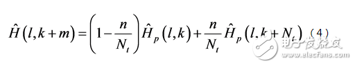
In order to reduce the limited multiplier resource consumption in the FPGA, the interpolation coefficient is calculated by input data shift calculation. Traditional interpolation estimation, the interpolation coefficient denominator is not ![]() When multipliers are used, the input data is multiplied by the interpolation coefficients previously stored in the ROM [7]. In this design, when the interpolation coefficient denominator is not
When multipliers are used, the input data is multiplied by the interpolation coefficients previously stored in the ROM [7]. In this design, when the interpolation coefficient denominator is not ![]() When selecting, add 8 bits of data decimal length in the lower bits of the data, and shift to calculate multiple data of the original data.
When selecting, add 8 bits of data decimal length in the lower bits of the data, and shift to calculate multiple data of the original data. ![]() In the first step, the high-order 16-bit data is obtained by adding the binary tree pipeline, and as shown in the formula (5) (6) (7) (8), the coefficient error is controlled at about 213.
In the first step, the high-order 16-bit data is obtained by adding the binary tree pipeline, and as shown in the formula (5) (6) (7) (8), the coefficient error is controlled at about 213.
3.3. Data processing module and output module
The MIMO transmit diversity scheme selects the space frequency coding of the LTE standard. When the MIMO decoding module performs maximum likelihood decoding, it is necessary to receive corresponding user data and channel parameters to construct a decision vector. According to the decision vector construction formula, it is known that each time the decision vector is constructed, two user data on two consecutive REs on the link and four channel channel parameters [11] are required to participate in the calculation. The data processing module serially combines the user data on two consecutive REs in the received two-layer link, and then outputs the data to the output module. The output module calculates the mean value of the channel parameters of the two RE addresses according to the received user data address, and outputs the same to the MIMO decoding module together with the user data.
3.4. Comprehensive testing and simulation
After modeling is complete, you need to synthesize on ISE. After synthesis, the resource consumption of the channel estimation module can be viewed in the ISE, as shown in Table 1.
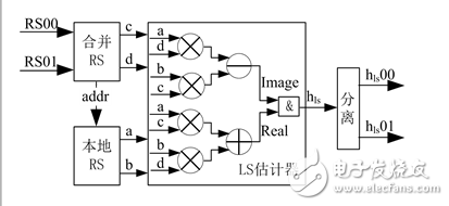
Figure 5. Architecture of LS esTImation module
Figure 5. Internal structure of the LS estimation module
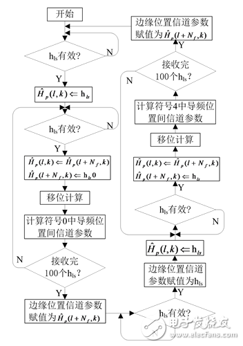
Figure 6. The flow chart of frequency domain interpolation
Figure 6. Frequency domain interpolation flow chart
After the success, the channel estimation module is added to the entire MIMO-OFDM physical transceiver link, and the data source is input at the transmitting end, and the simulation is performed by using Modelsim. In order to perform calculations on the FPGA, all data has been quantized into 16-bit fixed-point fractions, with the most significant bit being the sign bit, the next highest bit being the integer bit, and the remaining 14 bits being the decimal place, so the data range is between −2 and +2 . The channel parameter output is shown in Figure 8.
Despite the introduction of fixed-point and truncation errors in the data processing process, the fixed-point 16-bit data (CH00_OUT_RE and CH01_OUT_RE) of the channel parameters of channel 00 and channel 11 are still close to 16,384 (ie, 1). In a wired environment, since channel 01 and channel 10 do not receive data, the real and imaginary 16-bit data of the channel parameters are close to 0 (0). The input and output of the MIMO-OFDM baseband transmission link is as shown in FIG. 9, where the valid signal indicates data validity. After the sender (tx) of the data input link, the receiver (rx) output data is accurate and not lost. Therefore, the channel estimation module enables the system to correctly recover the data of the transmitter in a wired environment.
4. Video transmission testThe transmitting end and the receiving end of the designed physical layer link are respectively mounted as peripherals in the XPS project. Configure the Microblaze IP core in the ML605 development board to receive and encapsulate the video information sent by the video server on the sending end, and send it to the physical layer link through the logical channel; receive and parse the data information of the physical layer at the receiving end, and send it to the video. Decoder decoding. The Microblaze IP core and the physical layer link transmit data through the PLB (Processor Local Bus) bus. After the configuration is complete, download the generated bitstream file to the ML605.
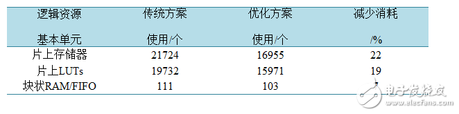
Table 1. Hardware resource consumption
Table 1. Hardware resource consumption
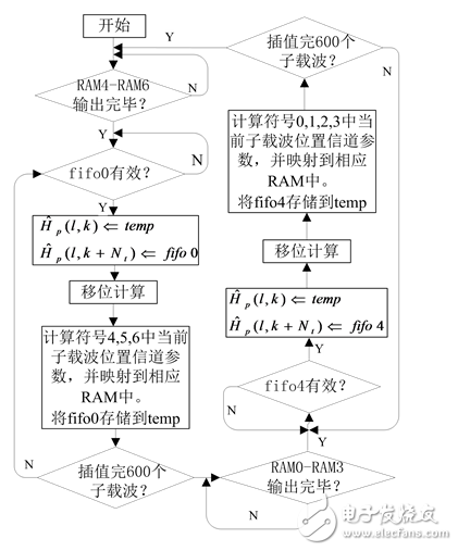
Figure 7. The flow chart of time domain interpolation
Figure 7. Time domain interpolation flowchart
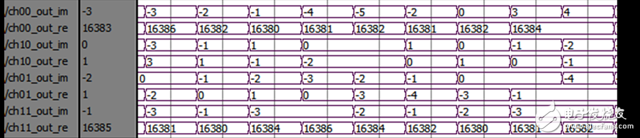
Figure 8. Simulation of channel parameters output
Figure 8. Channel estimation module channel parameter output simulation


Figure 9. Simulation of input and output of MIMO-OFDM link Figure 9. MIMO-OFDM link transceiving simulation
In the development board, the camera and the video server are set. After the video stream at the receiving end is decoded by the decoder, the video captured by the camera can be seen on the display, as shown in FIG. Two sets of equipment are placed in two adjacent laboratories, and the local camera can be seen to capture images and received
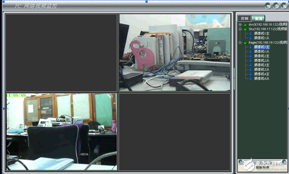
Figure 10. Video transmission test
Figure 10. Video transmission test
The image is clear and stable, which proves that the channel estimation module can effectively resist channel fading and improve system transmission reliability in a simple laboratory environment.
5 ConclusionIn this paper, for the MIMO-OFDM video transmission system, a LS algorithm and a linear interpolation algorithm are used to design a channel estimation scheme that consumes less logic resources of the FPGA, so that there is enough space on the FPGA chip to further the physical layer link. design. Supports up to 282.509 MHz clock frequency. After testing: After adding channel estimation, the video transmission system can perform wireless video transmission in a simple and fixed environment of the laboratory, and the image is clear and stable.
Lamp Post,powder coating Lamp Post,Garden Lamp Post,Steel Lamp Post,Galvanized Lamp Post
YIXING FUTAO METAL STRUCTURAL UNIT CO.,LTD( YIXING HONGSHENGYUAN ELECTRIC POWER FACILITIES CO.,LTD.) , https://www.chinasteelpole.com