Interpretation of IIC Bus FPGA Implementation Principle and Process
The IIC was developed in 1982 to provide easier interconnection of CPUs and peripheral chips in TVs. Television was one of the earliest embedded systems, and the original embedded system used memory-mapped I/O to interconnect microcontrollers and peripherals. To implement memory mapping, devices must be connected in parallel to the microcontroller's data and address lines. This approach requires a large number of lines and additional address decoding chips when connecting multiple peripherals, which is inconvenient and costly.
In order to save the pins of the microcontroller and additional logic chips to make the printed circuit board simpler and less expensive, the IIC (Inter-Integrated Circuit) was developed at the Philips laboratory in the Netherlands. It is composed of the data line SDA and the clock line. A serial bus consisting of two lines of SCL can send and receive data. Bidirectional transfer between the CPU and the controlled IC and IC and IC
IIC data transmission rate has standard mode (100kbps), fast mode (400kbps) and high-speed mode (3.4Mbps), while other variants achieve low-speed mode (10kbps) and fast+ mode (1Mbps)
IIC bus hardware structureIIC, I2C, is a bus structure.
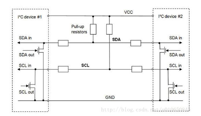
The internal SDA and SCL pin structure of each I2C bus device is the same. The pin's output drive is connected with the input buffer. The output is an open-drain FET and the input buffer is a high-input impedance non-inverting device. This circuit has two features:
Since SDA and SCL are open-drain structures, the signal's "AND-AND" logic is realized by means of an external pull-up resistor.
The pin can detect the level on the pin while outputting the signal, and check whether it is consistent with the output just now. Provides hardware infrastructure for "clock synchronization" and "bus arbitration."
Typical application of IIC equipment:
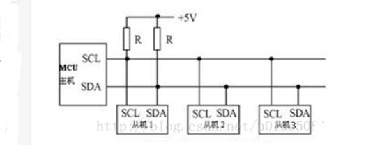
Physically, the IIC system consists of a serial data line SDA and a serial clock line SCL. The host addresses and transmits information to the slave according to a certain communication protocol. During data transmission, the host initiates a data transfer. The host transfers the data on the SDA line while also transmitting the clock through the SCL line. The object and direction of information transmission and the start and end of information transmission are determined by the host.
Each device has a unique address and can be a single-receiving device (for example, an LCD driver) or a device that can receive or transmit (for example, a memory). The transmitter or receiver can operate in master mode or slave mode, depending on whether the chip must initiate transmission of data or only addressed.
FPGA implementation principle and process of IIC bus I. Experimental platformSoftware Platform: ModelSim-Altera 6.4a (Quartus II 9.0)
Hardware platform: DIY_DE2
Second, the experimental principle1, IIC bus device working principle
The clock synchronization signal when transferring information on the IIC bus is accomplished by the logical AND of all devices attached to the SCL clock line. A high to low transition on the SCL line will affect these devices. Once a device's clock signal goes low, all devices on the SCL line will begin and protect the low period. At this time, a low-to-high transition of the clock of the device with a low low period does not affect the state of the SCL line, and these devices will enter a high-level wait state.
When the clock signal of all devices goes high, the low-level period ends and the SCL line is released back to high level, ie all devices start their high-level period at the same time. Afterwards, the first device that ends the high period pulls the SCL line low again. This generates a synchronous clock on the SCL line. It can be seen that the clock low time is determined by the device with the longest clock period, and the clock high time is determined by the device with the shortest clock period.
The data transfer rate on the IIC bus is up to 100 kbit/s in the standard mode and up to 400 kbit/s in the fast mode and up to 3.4 Mbit/s in the high speed mode. The number of interfaces connected to the bus is limited only by the 400 pF bus capacitance. Decision.
2, IIC bus transmission protocol and data transfer timing
(1) Start and stop conditions
During the data transfer process, the start and end of data transfer must be confirmed. In the IIC bus specification, the definitions of start and end signals (also called start and stop signals) are shown in Figure 1.
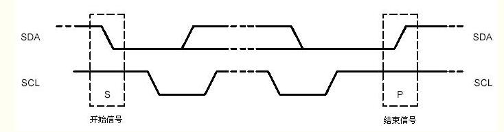
Figure 1 start and stop signal diagram
Start signal: When the clock bus SCL is high, the data line SDA transitions from high level to low level and starts to transmit data.
End signal: When the SCL line is high, the SDA line transitions from low to high, ending the transfer of data.
The start and end signals are generated by the master device. After the start signal, the bus is considered busy and no other device can generate a start signal. The master device exits the master role after completing the signal, and the bus is considered idle after a period of time.
(2) Data format
IIC bus data transmission adopts clock pulse serial transmission mode. During the low period of SCL, the high level and low level can change on the SDA line. During the high level, the data on the SDA must be protected and stabilized so that the receiver can sample the data. Receive, timing as shown in Figure 2.
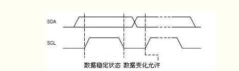
Figure 2 Data Transmission Timing Chart
Each byte sent by the IIC bus transmitter to the SDA line must be 8 bits long, with the high bit first and the low bit late. Correspondingly, the master device generates eight pulses on the SCL line; during the ninth pulse low period, the transmitter releases the SDA line, and the receiver pulls the SDA line low to give a receive acknowledgment bit; the ninth pulse During the high period, the transmitter receives this acknowledgment bit and then starts the transfer of the next byte. The receiver releases SDA during the first low pulse of the next byte. Each byte requires 9 pulses, and the number of bytes transferred each time is unlimited.
The IIC bus data transfer format is after the IIC bus start signal, the first byte of data sent is used to select the slave address, where the first 7 bits are the address code and the 8th bit is the direction bit (R/W). The direction bit is "0" to indicate that the master device writes information to the selected slave device; the direction bit to "1" indicates that the master device will read information from the slave device. The format is as follows:
After the start signal, each device in the system compares its own address with the address that the master device sends to the bus. If the address that the master device sends to the bus is the same, the device is the device addressed by the master device. Whether to receive information or send information is determined by bit 8 (R/W). The first byte is sent and the data signal is sent.
(3) Response
Data transmission must be responsive. The relevant response clock pulse is generated by the master. When the master device has transmitted one byte of data, it then issues an ACK acknowledge bit corresponding to the SCL line. During this clock, the master releases the SDA line and the one byte transfer ends. The slave response signal pulls the SDA line low, making SDA a stable low level during the high period of the clock. After the slave device's response signal ends, the SDA line returns high and goes to the next transmission cycle.
The normally addressed receiver must generate a response after each byte received. When the slave cannot respond to the slave address, the slave must keep the data line high and the master then generates a stop condition to terminate the transmission or generate a repeated start condition to start a new transmission. If the slave receiver responds to the slave address but cannot receive more data bytes after transmission, the master must terminate the transmission again. This condition is represented by the slave not generating a response after the first byte. The slave keeps the data line high and the master generates a stop or repeat start condition. The complete data transmission process is shown in Figure 3.
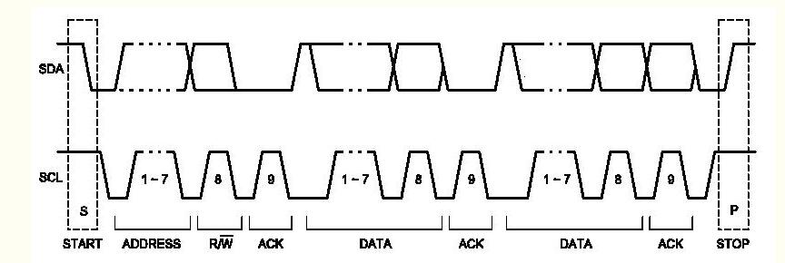
Figure 3 complete data transmission process
In addition, the IIC bus also has the function of broadcasting a call address for addressing all devices on the bus. If a device does not need to broadcast any data provided in the call addressing, then the address may be ignored. If the device needs to broadcast on-demand data in the call addressing, it should respond to the address, which appears as a receiver.
Third, the experimental processBased on the experimental principles described above, modelsim simulations are performed on the IIC part of the DE2_TV.
1, IIC clock simulation
As the host of the IIC device, the FPGA generates the IIC operating clock. The following first simulates the clock signals required by the IIC.
The clock signal program to be simulated is as follows:
Module I2C_Clock
(
iCLK,
iRST_N,
mI2C_CTRL_CLK,
mI2C_CLK_DIV,
mI2C_CLKO
);
Input iCLK;
Input iRST_N;
Output mI2C_CTRL_CLK;
Output mI2C_CLK_DIV;
Output mI2C_CLKO;
Reg mI2C_CTRL_CLK;
Reg [15:0] mI2C_CLK_DIV;
Reg mI2C_CLKO;
// Clock SetTIng
Parameter CLK_Freq = 50000000; //? ? ? 50 MHz
Parameter I2C_Freq = 80000; //? ? ? 40 KHz 25Us
Parameter I2C_Thd = 200000; //? ? ? 5Us 200 KHz
Always@(posedge iCLK or negedge iRST_N)
Begin
// 5000 TImes divide frequence of iCLK
If (!iRST_N)
Begin
mI2C_CLK_DIV << 0;
mI2C_CLKO << 0;
mI2C_CTRL_CLK <<= 0;
End
Else if( mI2C_CLK_DIV ((CLK_Freq/I2C_Freq))
Begin
mI2C_CLK_DIV "= mI2C_CLK_DIV+1;
If ((!!mI2C_CTRL_CLK)&(mI2C_CLK_DIV((CLK_Freq/I2C_Freq)-(CLK_Freq/I2C_Thd))) )
mI2C_CLKO << 0;
Else
mI2C_CLKO "= 1;
End
Else
Begin
mI2C_CLK_DIV << 0;
mI2C_CTRL_CLK << ~mI2C_CTRL_CLK;
End
End
Endmodule
The testbench program is as follows:
Module I2C_Clock_tb ;
//parameter I2C_Thd = 200000 ;
//parameter I2C_Freq = 80000 ;
//parameter CLK_Freq = 50000000 ;
Wire mI2C_CTRL_CLK ;
Wire [15:0] mI2C_CLK_DIV ;
Wire mI2C_CLKO ;
Reg iRST_N ;
Reg iCLK ;
I2C_Clock //#( I2C_Thd, I2C_Freq, CLK_Freq )
DUT (
.mI2C_CTRL_CLK (mI2C_CTRL_CLK) ,
.mI2C_CLK_DIV (mI2C_CLK_DIV) ,
.mI2C_CLKO (mI2C_CLKO ),
.iRST_N (iRST_N),
.iCLK (iCLK ) );
iniTIal
Begin
iRST_N = 0;
iCLK = 0;
#50
iRST_N = 1;
End
Always
Begin
#50 iCLK = ~iCLK;
End
Endmodule
The modelsim simulation waveform is as follows:
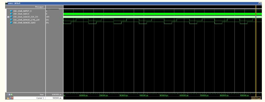
Figure 4 IIC internal clock simulation
After calculation, the internal clock frequency used by the IIC is 40KHz.
2, IIC overall simulation
Related procedures are in the attachment. The following is the simulation waveform.
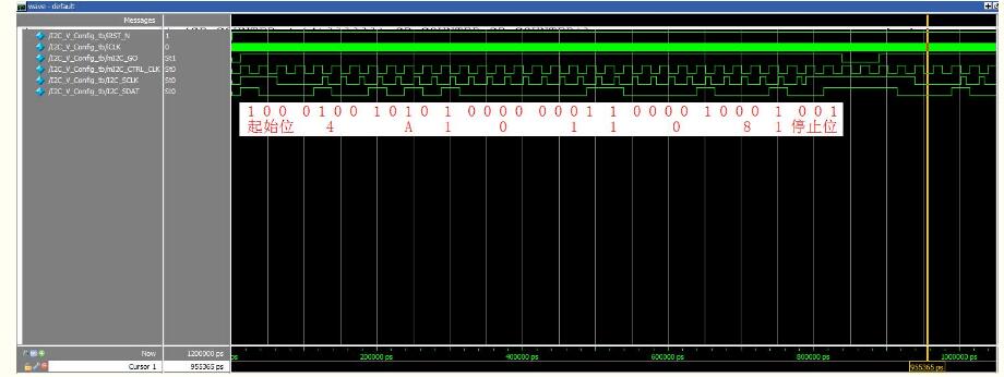
Figure 5 IIC overall simulation waveform
Combined with the above simulation waveform diagram and program can be seen:
Start bit: When SCLK is high, SDAT goes from high to low, indicating the start of the IIC bus transfer data;
After that, one byte of data is transmitted, namely 4A, which is the address of the slave, followed by a high level, which is the reply bit;
After that, one byte of data, ie, 01, is the subaddress of the slave address, followed by a high level, which is the reply bit.
After that, one byte of data, ie, 08, is transmitted for the above subaddress register, followed by a high level, which is the response bit.
Finally, for the stop bit, when SCLK is high, SDAT goes from low to high, indicating the end of the data transfer on the IIC bus.
From the simulation results, it can be seen that when one byte is transmitted, SDAT is a high pulse, instead of the SDAT pulling the device first and then pulling it high again.
Vacuum UV Curing Machine,Vacuum Curing Machine,UV Machine
Shenzhen Jianjiantong Technology Co., Ltd. , https://www.jjtphonesticker.com