Key issues and solutions for CDMA low noise amplifier design
Mobile communication technology is a product of the rapid development and integration of modern communication technology and computer technology. With the wide application of digital information technology, modern communication technology is developing at an unprecedented speed, and mobile communication is also developing along the direction of multiple access communication. Compared with FDMA (Frequency Division Multiple Access) and TDMA (Time Division Multiple Access), CDMA (Code Division Multiple Access) has the advantages of large system capacity, flexible configuration, high spectrum utilization, soft handover, and good security performance. Based on these advantages, CDMA technology has been widely used.
As the first stage of the CDMA receiver, the CDMA low noise amplifier directly determines the noise figure of the whole machine, which largely determines the receiver sensitivity. Therefore, a CDMA low noise amplifier with small noise figure, high gain, in-band flatness and high linearity becomes an important part of the CDMA transceiver.
Research and Design of CDMA Low Noise AmplifierBasic principles of CDMA low noise amplifier circuits
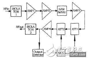
The functional block diagram of this low noise amplifier is shown in Figure 1. To meet the high gain of 50dB, the low noise amplifier uses four stages of amplification of AMP1, AMP2, AMP3 and AMP4; in order to get a good input-output standing wave ratio, the isolator ISOLATOR1 is used at the input and the isolator is used at the output. ISOLATOR2. In order to suppress various spurious signals outside the band, a SARFILTER acoustic surface filter with high suppression in this frequency band is used; in order to achieve gain adjustment, the numerical control attenuator ATT1 is used; in order to realize automatic control of output power, Voltage controlled attenuator ATT2.

Figure 1 CDMA low noise amplifier block diagram
The circuit can be divided into three small units: power processing circuit, monitoring processing circuit, and radio frequency (RF) link. The power processing circuit uses a Switching Power Supply LM7805 to convert the externally supplied 9V voltage to the 5V voltage required for each chip to operate. The LM7805 has high conversion efficiency and allows for a wide dynamic range of input voltage. The monitoring and processing circuit realizes RS485 communication interface with the host computer, output signal power detection, module gain adjustment and automatic level control (ALC).
The working principle of the RF link is shown in Figure 1. First, the input isolator ISOLATOR1 achieves good input standing wave ratio performance. The input signal is then amplified by two stages of AMP1 and AMP2, and then the out-of-band signal is suppressed by the surface acoustic wave filter SAW, and then amplified by the third stage of the AMP3. The gain-adjustable digital control attenuator ATT1 realizes the automatic level control voltage-controlled attenuator ATT2, and then passes through the AMP4 fourth-stage amplification. After AMP4, a small amount of energy is given to the detector to realize output power detection, and the main signal finally passes. Output isolator ISOLATOR2 output.
Key issues and solutions for CDMA low noise amplifier designDesign of low noise, high gain first and second stage amplifiers
According to the cascade equation of noise figure NFtot(m)=NF1+(N F2-1)/A v1+...+(N Fm-1)/Av1...A v(m-1) (where NFtot (m) is m-level total The noise figure, NFm is the noise figure of the mth level, and Avm is the gain of the mth stage.) The noise figure of the entire amplifier is mainly determined by the first stage and the second stage. The design of the first and second stage amplifiers with low noise and high gain is a difficult part of the overall low noise amplifier design. SAMP simulations of noise and gain were performed on AMP1 and AMP2 using Agilent's Advanced Design System (ADS). The results are shown in Figures 2 and 3.

Figure 2 AMPI noise and gain simulation results

Figure 3 AMP2 noise and gain simulation results
Portable high efficient travel charger, can charge multi devices at the same time, every port output mini 5v 1a, max 5v 2.1a. We can meet your specific requirement of the products, like label design. The plug type is US/UK/AU/EU. The material of this product is PC+ABS. All condition of our product is 100% brand new.
Our products built with input/output overvoltage protection, input/output overcurrent protection, over temperature protection, over power protection and short circuit protection. You can send more details of this product, so that we can offer best service to you!
Usb Charger,Universal Travel Adapter,Intelligent Usb Charger,Travel Adapter
Shenzhen Waweis Technology Co., Ltd. , https://www.szwaweischarger.com