Mobile video surveillance system solution based on 3G network
introduction
Today, with the rapid development of digital video surveillance technology, digital video surveillance systems are rapidly reaching out to various industries, such as enterprises, coal mines, schools, and public places, which have brought about a major change in people's work and life. With digital video, audio, voice and voice technology enabled in the DaVinci platform, DaVinci technology can lay the foundation for today's changes in digital video surveillance systems.
At the same time, with the opening of 3G networks, the HD mobile digital monitoring system provides the possibility of implementation.
The 3G mobile video surveillance system to be designed in this paper is a mobile real-time video surveillance system that can provide video capture, video data compression, linkage alarm, satellite positioning and network transmission. The main technical bottleneck lies in: 1 Whether the time consumption of its system can guarantee its real-time requirements, the key is that the H.264 compression algorithm takes time. Due to the limitations of embedded environment resources, in the case of real-time transmission of video data and image quality, especially in the case of multiple channels, it has not been guaranteed. However, with the maturity of DaVinci technology, its dual-core architecture of ARM 926EJ-S and DSP C64x+, H.264 compression algorithm runs independently on the Codec Server side of DSP, which solves the system's time-consuming guarantee of its real-time requirements. 2 Whether its 3G wireless network transmission can guarantee video quality and real-time. In terms of ensuring video quality and real-time transmission requirements, we can start from two aspects: 1 shorten the transmission time of video data, use the most efficient H.264 encoding technology to reduce the amount of information transmitted, and adopt dynamic adaptive adjustment of video data. Frame rate to reduce the amount of information transmitted to accommodate wireless bandwidth and jitter. 2 Realizing the QoS mechanism of video data transmission, designing and implementing the QoS mechanism of 3G wireless transmission, using the real-time transmission control protocol RTCP and RTP together, can optimize the transmission efficiency with effective feedback and minimum overhead, thus ensuring Video quality and its real-time nature.
1 system architecture and working principle
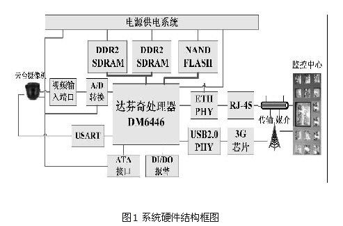
This system uses the DaVinci processor (TMS320DM6446), DDR2SDRAM (MT47H64M16), NAND FLASH (K9F1208X0C), video decoder TVP5150, 3G chip (ZTE MC8360), GPS satellite positioning chip plus peripheral interface chip. The CCD camera captures the analog video signal into the video decoder, performs analog-to-digital conversion, outputs a digital video signal conforming to the ITU-BT.656 standard, and then transmits the digital video signal to the front end of the video processing subsystem for pre-processing. The digital video signal is added to the black-end subtitles on the white background through the OSD subtitle adding algorithm designed by myself. After being coded by Codec Engine, it is sent to the 3G transmission chip through the USB2.0 bus port, and wirelessly transmitted to the remote video monitoring center; the Da Vinci processor detects The satellite positioning command is used to receive the GPS satellite positioning information through the serial port, and then the GPS satellite positioning information is transmitted to the 3G transmission chip, wirelessly transmitted to the remote video monitoring center, and the coordinate points and their movement tracks are calibrated on the map. The DSP side of the DM6446 is mainly responsible for video codec work, and the ARM side is used as a controller for controlling video decoding chip, 3G transmission chip, GPS positioning chip and peripheral interface chip. The system hardware block diagram is shown in Figure 1. 
2 hardware design
2.1 Video capture and decoding design
In this design, TI's video decoding chip TVP5150 is used to complete the analog/digital conversion of video images. The TVP5150 is an ultra-low-power, high-performance video decoder that supports NTSC/PAL/SECAM formats. It consumes only 115mW during normal operation and is available in a 32-pin TQFP ultra-small package. It can receive two CVBS or one S-Video signals and set its internal registers through the I2C bus to output 8-bit 4:2:2 ITU BT.656 signals.
The TVP5150 chip uses a 14.31818 MHz crystal oscillator as the input clock, the digital and analog input voltage is 1.8V, and the IO port voltage is 3.3V. The signal input has two channels, AIP1A and AIP1B, and both are impedance matched to prevent reflection of the input signal. YOUT[0:7] outputs 8 YcbCr signals, the line sync signal selects the pins HSYNC and VSYNC outputs; the SCLK pin outputs a 27MHz clock signal to the DM6446 chip for synchronous data acquisition.
2.2 DDR2 SDRAM memory interface design
Memory is mainly used to cache video input image data, store ARM and DSP code, and so on. DDR2 memory is a new type of high-speed, high-capacity dual-rate synchronous memory. Compared with DDR, DDR2 has higher bandwidth, lower power consumption and better high-speed performance.
This design uses Micron's MT47H64M16BT model DDR2 chip. The chip has a single-chip capacity of 1Gb and provides a 16-bit word length data bus interface. The chip uses 1.8V as the input voltage, and its memory supports differential latch signals, which can ensure the circuit is at high speed. In the case of accurate latching of the data on the bus, the system is more stable and reliable. In order to improve the system memory capacity and make maximum use of the 32 data bus of the DDR2 controller, two MT47H64M16BT are designed as the high and low 16 bits of the data bus to form a 32-bit data bus and a 256Mbyte memory system. When two 16-bit DDR2 chips are connected to the 32-bit bus DDR2 controller, the data bus and the corresponding data strobe signal and byte enable signal are respectively connected to the corresponding DDR2 chip, and the other signals are shared by two DDR2 chips. At this point, the DDR2 controller of the 32-bit data bus can access two DDR2 chips simultaneously.
2.3 Power supply design
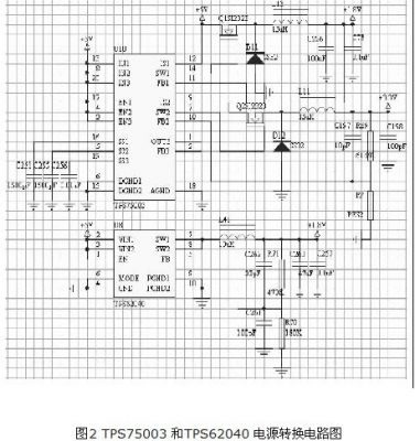
This design uses TI's TPS75003 and TPS62040 power management ICs. The TPS 7 5 0 0 3 has two maximum 3 A topology power supplies and one 300 mA LDO power supply. Each Buck output voltage ranges from 1.2V to 6.5V. The LDO output voltage ranges from 0.9V to 6.5V with an input voltage range of 2.2V to 6.5V. The TPS62040 is a high efficiency asynchronous switching DC/DC converter with a conversion efficiency of 95%, an input voltage range of 2.5V to 6.0V, and an output voltage of 0.7V to 6.0V, so it can be powered from mains +5V.
The system power supply is divided into four types: +5V, +3.3V, +1.8V, +1.2V. The main power supply of the system is +5V, and the rest are supplied by +5V power supply. Therefore, a TPS75003 and a TPS62040 are used to complete the conversion of the four power supplies of the system. The SW1 pin of the TPS75003 is designed to pass through the SI2323 free-wheel shaping and output 1.2V voltage for the DM6446 core. The IS1 pin is connected to the reference voltage, the FB1 pin is connected to the output 1.2V as the feedback, and the SW2 pin is outputting the 3.3V voltage. The DM6446 peripheral interface is powered. The SW1 and SW2 pins of the TPS62040 are shorted and output 1.8V for the DM6446 memory interface. The FB pin is connected to 1.8V as a feedback input. In this way, a TPS75003 and TPS62040 power management chip can be used to supply power to the system. The TPS75003 and TPS62040 power conversion circuits are shown in Figure 2. 
3 software solution design
This system uses embedded MontaVista Linux operating system platform, which is characterized by security, stability, high efficiency and high real-time. The system software of this paper adopts modular design. From the perspective of function, its software architecture is mainly divided into the following five parts: acquisition module, coding module, 3G transmission module, GPS satellite positioning module and equipment monitoring module. Since 3G wireless transmission is limited by its bandwidth, how to ensure video image quality and real-time performance is especially critical. Therefore, 3G transmission module is the core part of system software.
3.1 Acquisition Module
This module mainly completes video capture and image format conversion. Using V4L2 interface to capture the video data of the camera, V4L2 is a set of specifications for developing video capture device drivers under Linux. This set of specifications uses a layered approach to provide a clear model and consistent interface for driver development. The application is at the top, V4L2 is in the middle layer, and the hardware device is in the lower layer. Thus, through the driver, the application operates on the device as a file, shielding the specific operation of the hardware device.
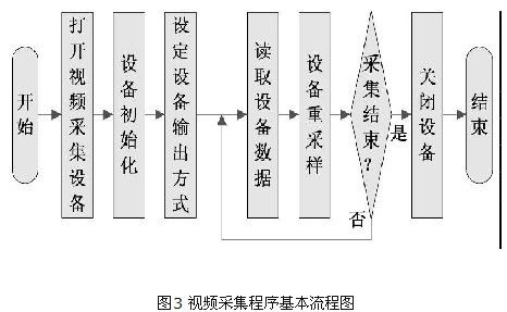
The TVP5150 driver is included in the Linux kernel. This design is based on the driver to implement video capture. The basic process of the video capture program is shown in Figure 3. 
3.2 Encoding module
This module mainly completes the addition of OSD subtitle information and the compression encoding of images.
The design makes full use of the Davinci codec engine interface for application programming. After YUV format conversion of the captured video data, the OSD subtitle algorithm is added to the OSD subtitle information by using the optimized TI company H.264 compression algorithm. Inter-code compression is performed on the processed YUV4:2:0 format data.
The OSD subtitle algorithm implements the addition of Chinese and English subtitle information on the YUV image, and can set the font's words and borders to two colors to clearly display the font under different background colors. The basic principle is to read the dot matrix data from the dot matrix font according to the ASCII character of the character, and perform a peripheral boundary pixel point expansion, so that the value of the corresponding bit of the adjacent 8 pixel points of 1 in each bit of the data can be determined. A value of 0 indicates that the point is the border of the character, and a value of 1 indicates that the point is the background color within the border of the character.
3.3 3G transmission module
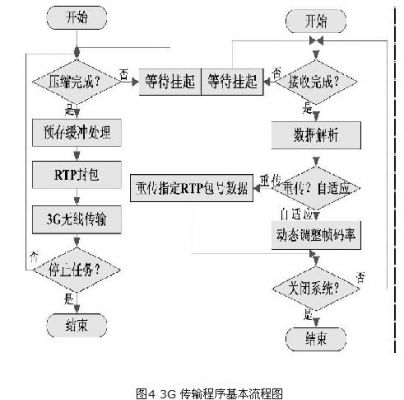
This part mainly completes 3G wireless network transmission of video data and system data, and is used to support functions such as video surveillance and system control communication. The RTP/RTCP protocol is used in the design. Due to the instability of the wireless network, the adaptive frame rate processing mechanism and QoS processing mechanism are added to ensure the video image quality and real-time requirements. The basic process is that after the compression coding is completed, the video pre-storage buffer processing is performed, and the encoded data is subjected to RTP packet processing, and then transmitted to the 3G module via the USB bus, and transmitted through the wireless network; after receiving the data, the command parsing process is performed to determine Whether there is an adaptive or retransmission control command to dynamically adjust the frame rate to reduce the wireless network transmission load, or to extract lost video data through a pre-stored buffer mechanism to complete the retransmission data transmission.
The basic flow of its 3G transmission program is shown in Figure 4. 
3.4 GPS satellite positioning module
The design uses the NMEA (National Marine Electronics Association) protocol of the GPS unified standard to complete the communication analysis. It mainly realizes the analysis and processing of the GPS satellite positioning data, and transmits it to the remote server software in real time to realize the 3G wireless mobile monitoring system platform. Position information, speed information, direction information, available satellite number and status information are displayed in real time, so that the geographic coordinates, movement trajectory and status information of the mobile platform are calibrated on the map.
3.5 Equipment Monitoring Module
This part mainly completes the system control command analysis and its response to realize the control of the PTZ, lens and other equipment; the detection and processing of various alarm events, such as video loss, video occlusion, motion detection alarm, etc.; system operation status Detection processing, to achieve automatic operation of system operation error or crash, automatic upgrade of system program, system program resetting factory settings, etc.; system operation authority and rule detection processing to achieve user privilege level management and operation rules Legalization.
4 Conclusion
The 3G wireless mobile video surveillance system has entered the internal testing phase and is powerful, stable, and scalable. It can perform video surveillance in 3G wireless bandwidth jitter, laying a solid foundation for mobile video surveillance applications, such as mobile. Police car monitoring system, etc. This paper proposes a design scheme of 3G mobile video surveillance system based on TI DM6446, and carries out detailed design of system hardware and detailed design of software modularization. The system solves the problem of adding OSD subtitle information and wireless bandwidth jitter in the front stage of video surveillance, so that video surveillance is smooth and stable.
This article refers to the address: http://
Av Over Ip System For Corporate Room
Av Over Ip System For Corporate Room,Video Decoder,Hd Video Decoder,Network Ip Decoder
SZ REACH TECH,.CO LTD , https://www.szreachtech.com