Reflow soldering technology
1. What is reflow soldering
Reflow is an English Reflow that softens the mechanical and electrical connection between the soldered end of the surface-mount component or the pin and the printed board pad by re-melting the solder solder pre-dispensed onto the pad of the printed board. Brazing. Reflow soldering is the soldering of components to PCB boards, and reflow soldering is done on the surface. Reflow soldering relies on the action of hot gas flow on the solder joint. The colloidal flux reacts physically under a certain high temperature airflow to achieve SMD soldering. The reason why it is called "reflow soldering" is because the gas flows in the welder to generate high temperature to reach the soldering. purpose.
The reflow soldering principle is divided into several descriptions :

(reflow soldering temperature graph)
A. When the PCB enters the heating zone, the solvent and gas in the solder paste evaporate. At the same time, the flux in the solder paste wets the pad, the component terminals and the leads, and the solder paste softens, collapses, and covers the solder. The disk isolates the pads and component leads from oxygen.
B. When the PCB enters the insulation zone, the PCB and components are fully preheated to prevent the PCB from entering the soldering high temperature zone and damaging the PCB and components .
C. When the PCB enters the soldering zone, the temperature rises rapidly and the solder paste reaches a molten state. The liquid solder wets, diffuses, diffuses or reflows the pads, component terminals and pins of the PCB to form solder joints.
D. The PCB enters the cooling zone to solidify the solder joint; the reflow soldering is completed.
How double-track reflow works
The dual-track reflow oven doubles the capacity of a single dual-track furnace by simultaneously processing two boards in parallel. Currently, board manufacturers are limited to processing boards of the same or similar weight in each track. Now, dual-track, two-speed reflow ovens with independent orbital speeds make it possible to process two more different boards simultaneously. First, we need to understand the main factors that affect the transfer of thermal energy from the reflow oven heater to the board. Under normal circumstances, as shown, the fan of the reflow oven pushes the gas (air or nitrogen) through the heating coil, and the gas is heated and passed through a series of orifices in the orifice to the product.
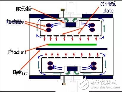
The following equations can be used to describe the transfer of thermal energy from the gas stream to the board, q = thermal energy transferred to the board; a = convective heat transfer coefficient of the board and components; t = board heating time; A = heat transfer surface area ΔT = temperature difference between convection gas and board We move the board related parameters to one side of the formula and move the reflow oven parameters to the other side to get the following formula: q = a | t | A | | T
The two-track reflow soldering PCB has become quite popular and has gradually become more and more popular. The main reason is that it gives designers a very good flexibility to design a compact, compact and low-cost design. product. To date, double-track reflow soldering plates have been soldered to the top (component side) by reflow soldering, and then soldered to the underside (pin side) by wave soldering. A current trend tends to double-track reflow solder reflow, but there are still some problems with this process. The bottom element of the slab may fall during the second reflow process, or the portion of the bottom solder joint may melt, causing solder joint reliability issues.
2. Introduction to reflow process
Reflow soldering is a surface-mounted board. The process is more complicated and can be divided into two types: single-sided mounting and double-sided mounting.
A, single-sided placement: pre-coated solder paste → patch (divided into manual placement and automatic machine placement) → reflow soldering → inspection and electrical testing.
B, double-sided mounting: A-side pre-coated solder paste → Patch (divided into manual placement and automatic machine placement) → Reflow soldering → B-side pre-coated solder paste → Patch (divided into manual placement and machine automatic Placement) → Reflow soldering → Inspection and electrical testing.
The simplest process of reflow soldering is "screen printing solder paste--sMD--reflow soldering. The core of the screen is accurate. The patch is determined by the machine's PPM. Reflow soldering is to control the temperature rise and maximum. Temperature and drop temperature curves.
Reflow soldering process requirements
Reflow soldering technology is no stranger to electronics manufacturing. The components on the various boards used in our computers are soldered to the board by this process. The advantage of this process is that the temperature is easy to control, oxidation can be avoided during the welding process, and manufacturing costs are easier to control. The inside of the device has a heating circuit that heats the nitrogen gas to a temperature high enough to blow the printed circuit board to the component, so that the solder on both sides of the component melts and bonds to the main board.
1. It is necessary to set a reasonable reflow soldering temperature curve and perform real-time testing of the temperature curve on a regular basis.
2. Weld according to the welding direction of the PCB design.
3. Strictly prevent belt vibration during welding.
4. The welding effect of the first printed board must be checked.
5. Whether the welding is sufficient, whether the surface of the solder joint is smooth, whether the shape of the solder joint is half moon, the condition of the solder ball and the residue, the case of continuous soldering and the solder joint. Also check the color change of the PCB surface and so on. And adjust the temperature curve according to the inspection results. The quality of the weld should be checked regularly during the entire batch.
Factors affecting the process:
1. Generally, PLCC and QFP have larger heat capacity than a discrete chip component, and it is more difficult to solder large-area components than small components.
2. In the reflow oven, the conveyor belt is reflowed in the same time, and it also becomes a heat dissipation system. In addition, the edge of the heating part is different from the central heat dissipation condition, and the edge is generally low in temperature, except for the temperature in each furnace. The temperature of the same surface is also different when the requirements are different.
3. The impact of different product loads. The adjustment of the reflow soldering temperature curve should take into account the good repeatability under no-load, load and different load factors. The load factor is defined as: LF = L / (L + S); where L = the length of the assembled substrate, and S = the spacing of the assembled substrates. Reflow soldering processes require reproducible results, and the greater the load factor, the more difficult it is. Generally, the maximum load factor of the reflow oven ranges from 0.5 to 0.9. This depends on the product (component solder density, different substrates) and the different models of the reflow oven. Practical experience is important to get good welding results and repeatability.
Reflow soldering is the core technology of the SMT process. All the electronic components on the PCB are completed by integral heating and one-time welding. The quality control of the SMT production line of the electronics factory is the absolute part of the work in order to obtain excellent welding quality. Set the temperature curve and manage the stove. This is something that all PEs know. A lot of literature and materials mention the setting of the reflow soldering temperature curve. For a new product, new furnace, new solder paste, how to quickly set the reflow soldering temperature curve? This requires us to have a basic understanding of the concept of temperature profiles and solder paste soldering principles.
In this paper, the most common lead-free solder paste Sn96.5Ag3.0Cu0.5 tin-silver-copper alloy is taken as an example to introduce the ideal reflow soldering temperature curve setting scheme and analyze its principle. Figure 1:
Figure 1 SAC305 lead-free solder paste reflow soldering temperature graph
Figure 1 shows a typical SAC305 alloy lead-free solder paste reflow soldering temperature profile. The six curves of yellow, orange, green, purple, blue and black are the temperature curves. Each point constituting the curve represents the temperature measured corresponding to the temperature measurement point on the PCB at the corresponding time during the furnace. By continuously recording the instantaneous temperature over time, by connecting these points, a continuously varying curve is obtained. It can also be seen as the process of changing the temperature of the test points on the PCB over time in the furnace.
Then, we divide this curve into four regions, and we get the time that the PCB has experienced in a certain area when it is reflowed. Here, we also want to clarify another concept "slope 1". The time taken to reflow an area by the PCB is divided by the absolute value of the temperature change during this period, and the resulting value is the "slope". The concept of introducing a slope is to indicate the rate at which the PCB heats up after heating, which is an important process parameter in the temperature profile. In the figure, four sections A, B, C and D are defined as A: heating zone, B: preheating zone (heat zone or activation zone), C: reflow zone (welding zone or Reflow zone), D: Cooling zone.
Continue to delve into the settings and meaning of the sections:
one. Warming zone A
The PCB enters the reflowed chain or mesh belt, and the area heated from room temperature to 150 °C is called the warming zone. The temperature rise zone is set at 60-90 seconds and the slope is controlled between 2-4.
The temperature of the components on the PCB board in this area rises relatively linearly, and the low-boiling solvent in the solder paste begins to partially evaporate. If the slope is too large and the heating rate is too fast, the solder paste will inevitably splash due to the rapid evaporation of the low boiling point solvent or the rapid boiling of the water vapor, thereby causing "tin bead" defects after the furnace. Excessive slopes can also cause mechanical damage such as micro-cracking of ceramic capacitors, deformation of PCB boards, and internal damage of BGA due to thermal stress.
Another negative consequence of too fast heating is that the solder paste cannot withstand a large thermal shock and collapses, which is one of the causes of the "short circuit". Long-term tracking of the service of the manufacturer, many manufacturers' SMT line the slope of the area actually controlled between 1.5-2.5 can get satisfactory results. Due to the different size and quality of the components mounted on each board, the temperature difference between the components at the end of the temperature rise zone is relatively large.
two. Preheating thermostat zone B
This area is also referred to as the insulation zone and activation zone in many literature and supplier literature.
The surface temperature of the PCB in this area rises gently from 150 ° C to 200 ° C, and the time window is between 60-120 seconds. The various parts of the PCB are slowly heated by hot air and the temperature rises slowly with time. The slope is between 0.3 and 0.8.
At this time, the organic solvent in the solder paste continues to volatilize. The active material is activated by temperature activation to remove oxides from the pad surface, the part feet, and the tin powder alloy powder. The purpose of the constant temperature rise in the constant temperature zone is to balance the temperature of the components of different sizes on the PCB. The temperature difference between components of different sizes and materials is gradually reduced, and the minimum temperature difference is reached before the solder paste is melted, ready for fusion welding in the next temperature zone. This is an important way to prevent "tombstone" defects. The activation temperature of the active agent in the SAC305 alloy solder paste formulation of many lead-free solder paste manufacturers is mostly between 150-200 °C, which is one of the reasons why the temperature curve preheats in this temperature range.
Need to pay attention to: 1, the warm-up time is too short. The reaction time of the active agent 3 with the oxide is insufficient, and the oxide on the surface of the solder is not effectively removed. The water vapor in the solder paste failed to evaporate completely slowly, and the low-boiling solvent volatilization amount was insufficient, which would cause the solvent to violently boil during soldering and splash to produce "tin beads". Insufficient wetting may result in poor "less tin", "short weld", "empty weld", and "leakage copper". 2. The warm-up time is too long. The active agent is over-consumed, and there is not enough active agent in the next temperature zone to melt and isolate the high temperature carbonized residue of the oxide and flux generated by the high temperature. In this case, the phenomenon of "virtual welding", "blackening of the residue", and "dark spot welding" may also be exhibited after the furnace.
three. Reflow pad C
The recirculation zone is also called the weld zone or the Refellow zone.
The melting point of SAC305 alloy is between 217 °C and 218 °C, so the region is >217 °C, the peak temperature is <245 °C, and the time is 30-70 seconds. The temperature at which high quality solder joints are formed is generally around 15-30 ° C above the melting point of the solder, so the minimum peak temperature in the reflow zone should be set above 230 ° C. Considering that the melting point of Sn96.5Ag3.0Cu0.5 lead-free solder paste is above 217 °C, in order to take care of PCB and components from high temperature damage, the peak temperature should be controlled below 250 °C. Most of the factory I have seen The peak temperature is below 245 °C.
After the preheating zone is over, the temperature on the PCB rises to the liquidus of the tin powder alloy at a relatively fast rate. At this point, the solder begins to melt and continues to linearly warm up to the peak temperature and then begins to fall to the solidus line after a period of time.
At this point, the various components of the solder paste function fully: the rosin or resin softens and forms a protective film around the solder that is isolated from oxygen. The surfactant is activated to reduce the surface tension between the solder and the surface to be soldered, and to enhance the wetting force of the liquid solder. The active agent continues to react with the oxide, continuously removing oxides and carbides produced by the high temperature and providing partial fluidity until the reaction is completely completed. Some of the additives decompose and volatilize at high temperatures without leaving a residue. The high boiling solvent evaporates over time and completely evaporates at the end of reflow. The stabilizer is evenly distributed in the metal and the solder joint surface protects the solder joint from oxidation. The solder powder is converted from a solid to a liquid and spreads as the solder wets. A small amount of different metals undergo a chemical reaction to produce intermetallic compounds. For example, a typical tin-silver-copper alloy has Ag3Sn and Cu6Sn5.
The reflow zone is the most central section of the temperature profile. The peak temperature is too low and the time is too short. The liquid solder does not have enough time to flow and wet, resulting in “cold weldingâ€, “virtual weldingâ€, “poor infiltration (leakage)â€, “not bright solder joints†and “more residueâ€. "Other defects; peak temperature is too high or too long, causing defects such as "PCB board deformation", "component thermal damage", "black residue" and so on. It requires a balance between the peak temperature, the upper temperature limit and time that the PCB and components can withstand, and the melting time that results in the best soldering effect, in order to achieve the desired solder joint.
four. Cooling zone D
The section where the solder joint temperature is lowered downward from the liquidus is referred to as a cooling zone. Typically, the cooling zone of SAC305 alloy solder paste is generally considered to be between 217 ° C and 170 ° C (some literatures suggest a minimum of 150 ° C).
Since the liquid solder is cooled below the liquidus to form a solid solder joint, the quality after solder joint formation cannot be judged by the naked eye in a short period of time, so many factories often do not pay much attention to the setting of the cooling zone. However, the cooling rate of the solder joints is related to the long-term reliability of the solder joints and cannot be taken seriously.
The main point of control of the cooling zone is the cooling rate. After many solder laboratory studies, the conclusion is that rapid cooling is beneficial to obtain stable and reliable solder joints.
Usually people's intuition that it should be slowly cooled to offset the thermal shock of various components and solder joints. However, reflow solder paste brazing slow cooling will form more coarse grains, and larger intermetallic compound particles such as Ag3Sn and Cu6Sn5 will be formed in the interface layer and inside of the solder joint. Reduce the mechanical strength and thermal cycle life of the solder joint, and it may cause the solder joint to have low gloss or even dullness.
Rapid cooling can form smooth, uniform and thin intermetallic compounds, forming fine tin-rich dendrites and fine grains dispersed in the tin matrix, which can significantly improve and improve the mechanical properties and reliability of the solder joints.
In production applications, the greater the cooling rate, the better. It should be considered in combination with the cooling capacity of the reflow soldering equipment, the thermal shock that the board, components and solder joints can withstand. A balance should be sought between the board and the components without sacrificing solder joint quality. The minimum cooling rate should be above 2.5 °C and the optimal cooling rate is above 3 °C. Considering the thermal shock that components and PCBs can withstand, the maximum cooling rate should be controlled at 6-10 °C. When selecting equipment, the factory should choose reflow soldering with water cooling function to obtain a strong cooling capacity reserve.
3. What are the advantages of reflow soldering technology?
1) When reflow soldering technology is used for soldering, the printed circuit board does not need to be immersed in the molten solder, but the local heating is used to complete the welding task; thus the soldered components are less affected by thermal shock and are not caused by overheating. Damage to components.
2) Since the soldering technique only needs to apply solder at the soldering portion and locally heat the soldering, welding defects such as bridging are avoided.
3) In the reflow soldering technology, the solder is only used once and there is no reuse. Therefore, the solder is pure and has no impurities, which ensures the quality of the solder joint.
4. Reflow soldering precautions
1. Bridge reflow soldering will also produce solder sag during heating. This occurs in both preheating and main heating. When the preheating temperature is in the range of tens to a hundred degrees, it is one of the components in the solder. The solvent will lower the viscosity and flow out. If the tendency of the solvent is very strong, the solder particles will be extruded out of the gold-containing particles outside the soldering zone, and if it cannot be returned to the soldering area during melting, the retained solder will be formed. ball. In addition to the above factors, whether the terminal electrode of the SMD component is flat, whether the wiring layout of the circuit board and the spacing of the pad are standardized, the selection of the solder resist coating method and the coating accuracy thereof are the causes of the bridge. 2. The monumental element floats (Manhattan phenomenon). The chip component is tilted under the condition of rapid heating by reflow soldering . This is because the heat is applied to the temperature difference between the two ends of the device, and the solder on the electrode side is completely melted. Wet, while the other side of the solder is not completely melted, causing poor wetting, which promotes the erection of the component. Therefore, when reflow soldering is heated, it is necessary to form a balanced temperature distribution from the viewpoint of time elements to avoid the generation of rapid heat of reflow soldering . The main factors preventing the component from erecting are as follows: 1. Selecting a solder with strong bonding force, the printing precision of the solder and the mounting accuracy of the component also need to be improved; 2 The external electrode of the component needs to have good wettability and wet stability. . Recommended: temperature below 40 °C, humidity below 70% RH, the use period of incoming components can not exceed 6 months; 3 use small weld width dimension to reduce the surface tension generated on the end of the component when the solder melts. In addition, the printing thickness of the solder can be appropriately reduced, for example, 100 μm is selected; 4 The setting of the welding temperature management condition is also a factor of the component erection. The usual goal is to heat evenly, especially before the weld fillet at the two joint ends of the component is formed, the equalization heating must not fluctuate. 3. Poor wetting The poor wetting is the soldering of the solder and the circuit board (copper foil) or the external electrode of the SMD during the reflow soldering process. After the wetting, the mutual reaction layer is not formed, resulting in leakage or less soldering. malfunction. Most of the reasons are caused by the contamination of the surface of the soldering area or by the solder resist, or by the formation of a metal compound layer on the surface of the bonded object. For example, the surface of silver has sulfides, and the surface of tin has oxides which cause poor wetting. When the amount of aluminum, zinc, cadmium or the like remaining in the solder exceeds 0.005% or more, the degree of activation is lowered by the moisture absorption of the flux, and poor wetting may occur. Therefore, anti-fouling measures should be taken on the surface of the soldered substrate and the surface of the component. Choose the right solder and set a reasonable soldering temperature profile for reflow soldering . Five steps for lead-free soldering: 1 Choosing the right materials and methods In the lead-free soldering process, the choice of solder material is the most challenging. Because of the lead-free soldering process, the choice of materials such as lead-free solder, solder paste, flux, etc. is the most critical and most difficult. The choice of these materials also takes into account the type of soldering elements, the type of board, and their surface coating. The materials selected should be proven in their own research, or recommended by an authority or literature, or have been used. These materials are tabulated for testing in process trials to conduct in-depth studies to understand their impact on various aspects of the process. For the welding method, it is necessary to choose according to its actual situation, such as component type: surface mount component, through-hole insert component; circuit board condition; the number and distribution of components on the board. For the soldering of surface mount components, reflow soldering is required; for via reflow soldering components, wave soldering, dip soldering or spray soldering may be selected for soldering. Wave soldering is more suitable for the soldering of the through-hole component on the whole board (large); dip soldering is more suitable for reflow soldering of the through-hole component on the whole board (small) or on the board ; local spray solder It is more suitable for reflow soldering of individual components on board or a small number of through-hole components . In addition, it should be noted that the whole process of lead- free reflow soldering is longer than that of lead-containing solder, and the required soldering temperature is higher because the melting point of lead-free solder is higher than that of lead-containing solder. The infiltration is worse because of the infiltration. After the welding method is selected, the type of welding process is determined. At this time, it is necessary to select equipment and related process control and process inspection instruments according to the welding process requirements, or to upgrade. The choice of welding equipment and related equipment is as critical as the choice of welding materials. 2 Determination of process route and process conditions After the first step is completed, the welding process can be tested on the selected welding materials. The process route and process conditions are determined experimentally. In the test, the selected welding materials need to be fully tested to understand their characteristics and impact on the process. The purpose of this step is to develop samples for lead-free soldering. 3 Develop and improve the welding process This step is the continuation of the second step. It analyzes the test data collected in the second step of the process test to improve the materials, equipment or process to obtain a sound process under laboratory conditions. In this step, it is necessary to clarify the possible processability (CPK) values ​​of the lead-free alloy soldering process, how to prevent and measure various soldering characteristics, and compare it with the original tin/lead process. Through these studies, it is possible to develop inspection and testing procedures for the welding process, as well as to find out how to handle the process out of control. 4. A reliability test of the weld sample is also required to verify that the quality of the product meets the requirements. If the requirements are not met, the cause should be identified and resolved until the requirements are met. Once the reliability of the soldered product meets the requirements, the development of the lead-free soldering process has been successful. This process is ready for mass production and ready for operation. Now it can be transformed from sample production to industrial production. At this point, the process still needs to be done to keep the process under control. 5 Control and Improvement Process The lead-free soldering process is a dynamic stage. Factories must be alert to possible problems to avoid process runaway, as well as continually improve the process to improve product quality and acceptable crystallinity. For any lead-free soldering process, improved soldering materials and newer equipment can improve the solderability of the product.
Guangdong Kaihua Electric Appliance Co., Ltd. , https://www.kaihuacable.com