Unveil the mystery of the Zynq Z-7000 flash boot from the SPI interface
When developing FPGA products, you not only need to be familiar with the hardware on the board, but also run the code on the hardware. You want to observe the operation of the code on the hardware through the hardware analyzer of the logic analyzer. Digital Discovery with built-in Xilinx Spartan-6 FPGA provides high-speed logic analysis that allows developers to observe and analyze the signal flow on the board. At the same time, we introduce Zinq Z-7000 SoC to another Xilinx chip today. Let's uncover the mystery of the flash boot that it mounts from the SPI interface.
The Zynq board is booted from the flash of the SPI port using Digilent's Digital Discovery. There are two reasons to use Digital Discovery instead of a logic analyzer. First, QSPI transmission is performed at a higher clock frequency. In this case, it is likely to exceed 100MHz, so a higher sampling rate is required. Secondly, With 512 MB of DDR, Digital Discovery can store more samples of the collected signals. So, with so many theories, do you already want to know how to connect Digital Discovery and Zynq together? The specific connection method is shown in Figure 1. The digital sampling port of Digital Discovery is connected to the corresponding pin of Zynq's falsh chip, and then Digital Discovery is connected to the PC via USB, and the signal is transmitted by the host computer Waveforms. Collection and processing.
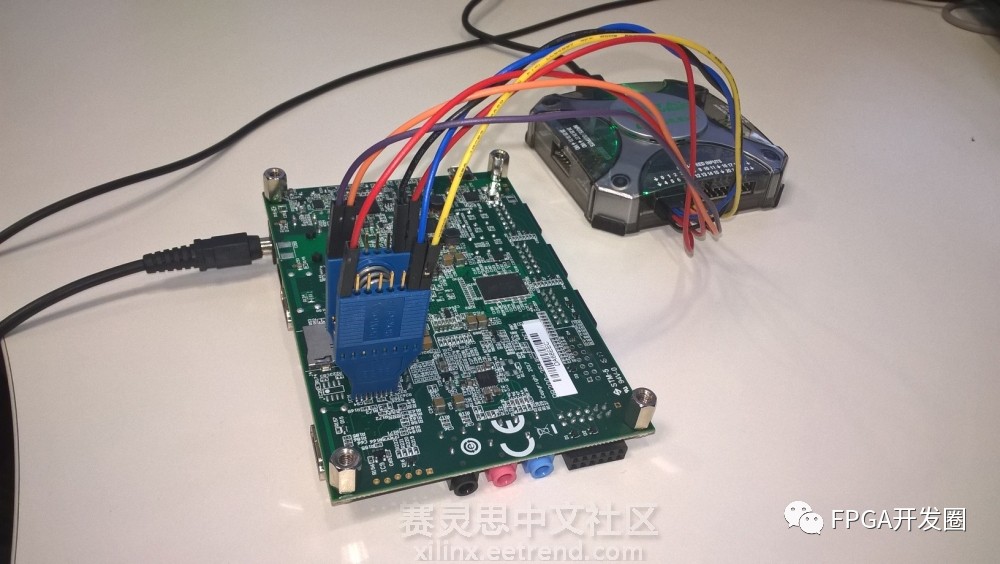
Fig. 1 Connection method for capturing the start signal of Zynq Z-7000 SoC with Digital Discovery logic analyzer
The maximum QSPI clock frequency is about 100MHz. When starting up, the overall startup time is about 700ms, which requires a large sampling rate. Digital Discovery can support such frequencies, and 2.68 million instructions need to be transmitted under 200MHz. 1.3 seconds. The sampling is triggered on the falling edge of the CS signal. The sampling of the data requires a large amount of computer memory, and the processing time is relatively long. Fig. 2 shows the transmission waveform of the overall QSPI. Note that the frequency of the leftmost clock of the obtained waveform has changed from 5.4 MHz to 25 MHz.
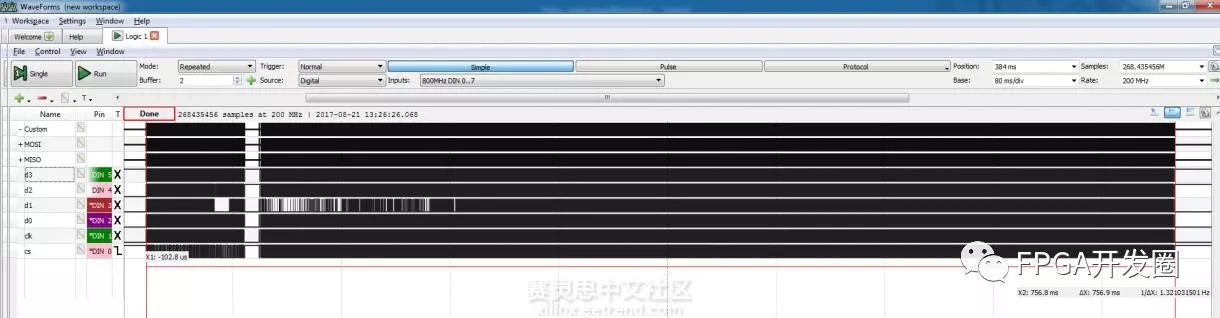
Fig. 2 Digilent's Digital Discovery Logic Analyzer captures the entire process of Zynq Z-7000 startup
If you want to understand what the data transfer means, you can refer to the Zynq TRM and the corresponding flash data sheet. The instruction is transferred from Zynq to flash through the D0 pin of SPI. The first instruction sends 0x03 0x00 0x00 0x20 (the red box part of Fig. 3). This instruction means SPI READ, the read address is 0x20; Correspondingly, the received reply signal is obtained through the SPI D1 pin, and the received signal is 0x66 0x55 0x99 0xaa (shown in the blue box of Figure 3.), explained in pages 170 to 179 of Zynq TRM. The received signal means that flash tells Zynq that this flash supports QSPI. It is observed that the clock frequency of the SPI is 5.405MHz in the place where the instruction is read, and the frequency of this clock is relatively low. After the read command, flash supports QSPI and all transfers are performed on four QSPI data lines. The next instruction is 0x6b, followed by a physical address of 3 bytes, as shown in the red box in Figure 4. The 0x6b represents four read and write instructions, and the flash response data is after 8 clock cycles (Fig. 4 The middle green box is shown) can be observed on the QSPI signal line, as shown in the blue box in Figure 4.
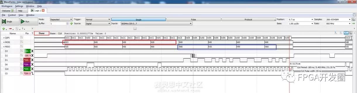
Fig. 3 The first read signal command sent by Zynq to flash and the feedback signal waveform of flash
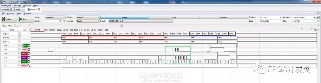
Fig. 4 Zynq's four read and write instructions and the corresponding QSPI signals
The Zynq-7000 AP SoC integrates an ARM processor core and a hardware-programmable FPGA. It integrates a CPU, DSP, ASSP, and mixed-signal processing device on a single chip and can be used for major data analysis and hardware acceleration. Has a very good performance and price ratio. Digital Discovery uses Xilinx's Spartan-6 FPGA, which has a high logic-to-pin ratio, built-in MicroBlaze soft core, supports 800Mb/s DDR3, supports rich I/O protocol, so performance can Competent for the work of logic analyzers.
It's not surprising to use a logic analyzer to capture the signal waveforms at the start of the processor, but in this case the Digital Discovery logic analyzer function is used. The highlight is the interaction of the two chips from Xilinx. The start signal reveals a trip. Both Digital Discovery and Zynq SoC are excellent products. One is the hardware developer's portable debugging magic, and the other is the hardware developer's high-performance development board. Do you want to try it yourself?
Photo Studio Kit,Photography Lighting Kit,Photography Studio Kit,Photography Studio Lighting Kit
SHAOXING SHANGYU FEIXIANG PHOTOGRAPHIC CO.,LTD , https://www.flying-photography.com