What is the introduction of the structure and key parameters of MOSFET and its application prospects?
Recently, the domestic demand for MOSFETs has soared, leading to a shortage of goods in the industry. Many manufacturers have money and cannot buy them. This is what MOSFET manufacturers are most willing to see. The growth in MOSFET demand stems from the rapid development of the Internet of Things, 3C products, cloud computing and servers.
MOSFET is also called metal-oxide semiconductor field effect transistor, or MOSFET for short. It is a field effect transistor that can be widely used in analog circuits and digital circuits. MOSFETs can be divided into two types: "N-type" and "P-type" according to the polarity of their "channels". They are usually also called NMOSFET and PMOSFET, and abbreviations include NMOS, PMOS, etc. This article takes everyone to familiarize yourself with the structure and prospects of MOSFETs.
MOSFET structure
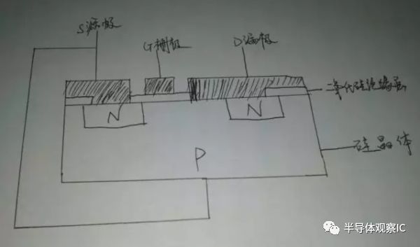
The figure above is a cross-sectional view of a typical planar N-channel enhancement mode NMOSFET. It uses a P-type silicon semiconductor material as a substrate, diffuses two N-type regions on its surface, and then covers a layer of silicon dioxide (SiO2) insulating layer, and finally it is made by etching above the N-region Two holes, using metallization method to make three electrodes on the insulating layer and in the two holes: G (gate), S (source) and D (drain).
It can be seen from the figure that the gate G is insulated from the drain D and the source S, and there are two PN junctions between D and S. Under normal circumstances, the substrate and the source are connected together internally, which is equivalent to a PN junction between D and S.
Figure 1 is a basic structure diagram of a common N-channel enhancement MOSFET. In order to improve the characteristics of certain parameters, such as increasing the working current, increasing the working voltage, reducing the on-resistance, and improving the switching characteristics, there are different structures and processes to form the so-called VMOS, DMOS, TMOS and other structures.
MOSFET key parameters
There are many parameters of MOSFET, including DC parameters, AC parameters and limit parameters, but generally pay attention to the following main parameters:
1. IDSS—Saturated drain-source current. It refers to the drain-source current when the gate voltage UGS=0 in the junction or depletion insulated gate field effect transistor.
2. UP—Pinch off voltage. It refers to the gate voltage when the drain-source is just cut off in the junction or depletion-type insulated gate field effect transistor.
3. UT—Turn on the voltage. It refers to the gate voltage when the drain source is just turned on in the enhanced insulated gate field effect transistor.
4. gM—transconductance. It represents the gate-source voltage UGS—the ability to control the drain current ID, that is, the ratio of the change in the drain current ID to the change in the gate-source voltage UGS. gM is an important parameter to measure the amplification ability of the field effect tube.
5. BUDS—Drain-source breakdown voltage. It refers to the maximum drain-source voltage that the FET can withstand when the gate-source voltage UGS is constant. This is a limit parameter, and the working voltage applied to the FET must be less than BUDS.
6. PDSM—Maximum power dissipation. It is also a limiting parameter, which refers to the maximum allowable drain-source power dissipation when the performance of the field effect tube does not deteriorate. When in use, the actual power consumption of the field effect tube should be less than that of the PDSM and leave a certain margin.
7. IDSM—Maximum drain-source current. It is a limit parameter, which refers to the maximum current allowed to pass between the drain and the source when the FET is working normally. The working current of the FET should not exceed IDSM.
MOSFET market prospects
The continuous improvement of microprocessor computing performance brings more power to the in-depth research and development of a new generation of MOSFET, which also makes the operation speed of MOSFET itself faster and faster, almost becoming the fastest of various semiconductor active components. The main success of MOSFET in digital signal processing comes from the invention of CMOS logic circuit. The biggest advantage of this structure is that there is no static power loss in theory, and current flows only when the logic gate is switched. The most basic member of CMOS logic gates is a CMOS inverter, and the basic operation of all CMOS logic gates is the same as that of an inverter. At the moment of logic conversion, only one type of transistor must be in the conducting state at the same time. One must be the cut-off state, which makes there is no direct conduction path from the power terminal to the ground terminal, which saves a lot of current or power consumption, and also reduces the heat generation of the integrated circuit.
Another major advantage of MOSFETs in digital circuits is that for DC signals, the impedance of the MOSFET's gate terminal is infinite, that is, theoretically, no current flows from the gate terminal of the MOSFET to the ground point in the circuit, but completely The form of the gate is controlled by the voltage. This makes MOSFETs more power efficient and easier to drive than their main competitor BJT.
In CMOS logic circuits, in addition to the drivers responsible for driving the off-chip load, the logic gates of each level only need to face the gate of the same MOSFET, so that the driving force of the logic gate itself is less need to be considered. In contrast, BJT's logic circuit does not have these advantages. The infinite gate input resistance of the MOSFET also has other advantages for the circuit design engineer, for example, it is less necessary to consider the load effect at the output of the logic gate.
Acrylic Anti Blue Light Filter
Acrylic Anti Blue Light Filter,Blue Light Screen Protectors,Anti Blue Light Filter,Blue Light Filter For Pc
Guangdong magic Electronic Limited , https://www.magicmax.cc