Basic knowledge of FPGA (Field Programmable Gate Array) and how it works
High-end design tools provide field-programmable gate arrays (FPGAs) for engineers and scientists with few hardware design techniques. Whether you use a graphical design program, ANSI C or VHDL, such a complex synthesis process can not help but think about the real operation of the FPGA. How the program in this chip works between these settable silicon chips. This book will make non-digital designers understand the basics of FPGA (Field Programmable Gate Array) and how it works. This information is also very useful when using high-end design tools, and hopefully provides some clues for understanding this particular technology.
1. FPGA-Field Programmable Gate ArrayEach FPGA chip is composed of a limited number of predefined sources with programmable connections to implement a reconfigurable digital circuit.
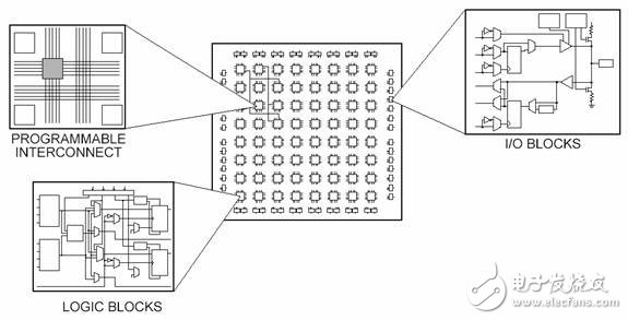
Figure 1. Different components of FPGA
The FPGA chip specification includes the number of programmable logic blocks, the number of fixed function logic blocks (such as multipliers), and the size of memory resources (such as embedded RAM). There are many other parts in the FPGA chip, but the above indicators are usually the most important reference when selecting and comparing FPGAs for specific applications.
At the bottom, configurable logic blocks (such as slices or logical units) have two basic components: triggers and lookup tables (LUTs). This is important because the various FPGA families are different because of the different ways in which triggers and lookup tables are combined. For example, the Virtex-II family of FPGAs has two look-up tables and two flip-flops, while the Virtex-5 FPGA has four look-up tables and four flip-flops. The structure of the lookup table itself may also vary (4 inputs or 6 inputs). More information on how the lookup table works will be given in the following sections.
Table 1 lists the metrics for the FPGAs used in the NI LabVIEW FPGA hardware target. The number of logic gates is a traditional method of comparing FPGA chips to ASIC technology, but it does not truly represent the number of independent cells inside the FPGA. This is one of the reasons why Xilinx did not specify the number of logic gates in the new Virtex-5 family.
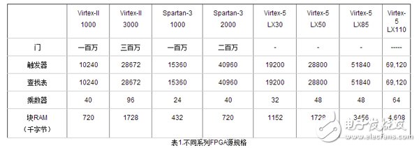
Table 1. Different series of FPGA source specifications
To better understand the meaning of these specifications, the coding is considered a composite digital circuit mode. For any piece of synthetic code, or graphical or textual form, there is a corresponding circuit diagram that reflects how the logical components should be wired. The corresponding schematic diagram is understood by a simple Boolean logic circuit. Figure 2 shows a functional group that passes 5 Boolean signals and can graphically calculate the resulting binary values.
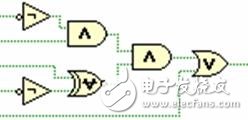
Figure 2. Simple Boolean logic for loading 5 signals
Under normal circumstances (outside LabVIEW SCTL - single-cycle timing loop), the corresponding circuit diagram shown in Figure 2 is similar to that shown in Figure 3.
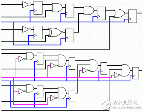
Figure 3. Corresponding circuit diagram of Boolean logic in Figure 2.
Although it is difficult to understand, in reality, two parallel branch circuits are created here. The top five black lines are fed back to the first branch, which adds a trigger between each Boolean operation. The bottom five black lines form the second logical chain. One of the paths adds a synchronization register between each step, and the other logical chain ensures that the data stream is executed. A total of 12 flip-flops and 12 look-up tables are required for this circuit diagram to work properly. The upper branch and each component will be analyzed in a later chapter.
2. Trigger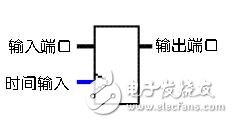
Figure 4. Trigger symbol
A flip-flop is a binary shift register that is used to synchronize logic and save logic state during a clock (pulse) cycle. At each time (pulse) edge, the flip-flop locks a 1 (true) or 0 (false) value on input and saves this value until the next clock (pulse) edge. Under normal circumstances, LabVIEW FPGA sets a trigger between each operation to ensure that there is enough time to perform each step. The exception to this law only occurs when writing code in the SCTL structure. In this particular loop structure, the flip-flop is placed only at the beginning and end of the closed-loop iteration, and the programmer considers the timing factor to determine how to place it. More on how the code within the SCTL is synchronized will be discussed in a later chapter. Figure 5 shows the upper branch of Figure 3 with the trigger highlighted in red.
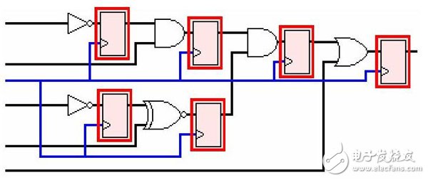
Figure 5. Draw a circuit diagram showing the trigger highlighted in red
3. Lookup table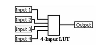
Figure 6. Dual four-input lookup table
The other logic in the diagram shown in Figure 6 is implemented by using a random access memory in the form of a small number of lookup tables. We can simply assume that the number of system gates in an FPGA can refer to the number of NAND gates (NAND) and NOR gates, but in fact, all combinatorial logic (AND gate, OR gate, NAND gate, XOR) Gates, etc. are all implemented by looking up the truth table in the table memory. The truth table is a predefined table that outputs a combination of each input value (the importance of the Karnaugh map may fade in your mind). The following is a quick review of the digital logic circuit course: for example, Figure 7 is a Boolean logic and gate operation process.
This is a quick review of the digital logic course:
For example, a Boolean AND operation is shown in FIG.
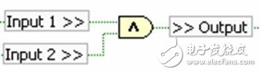
Figure 7. Boolean AND operation
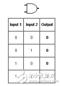
Table 2. Truth Table for Boolean and Gate Operations
You can think of the input value as a numeric index of all output values, as shown in Table 3.
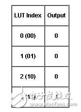
Table 3. Reality lookup table implementation for Boolean and gate wipe operations
The Virtex-II and Spartan-3 family of FPGA chips have a 4-input lookup table to achieve 16 combinations of true 4-input signals. Figure 8 is an example of a four-input circuit implementation.
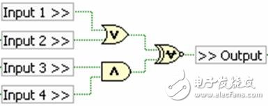
Figure 8. Four-signal circuit with input Boolean logic
Table 4 shows the corresponding truth table implemented using the dual four-input lookup table.
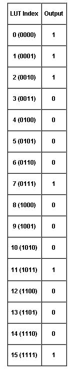
Table 4. Corresponding truth table shown in Figure 8.
The Virtex-5 family of FPGAs uses a dual six-input lookup table that implements a truth table with 64 combinations of six different input signals. Because the combinational logic between flip-flops is complex, it is increasingly important to use SCTL in LabVIEW FPGA. The next section describes how SCTL optimizes the use of FPGA sources in LabVIEW.
4. SCTLThe code examples used in the previous sections assume that the code is set outside of the SCTL and that additional circuitry is synchronized to ensure that the amount of synchronized data is executed. SCTL is a special structure in LabVIEW FPGA that produces a more optimized circuit diagram in the hope of performing all logic branching in one clock (pulse) cycle. For example, if the SCTL is set to run at 40 MHz, all logic branches will be executed in 25 ns.
If the same Boolean logic circuit as in the previous example is set in the SCTL (as shown in FIG. 9), a corresponding circuit diagram as shown in FIG. 10 is generated.
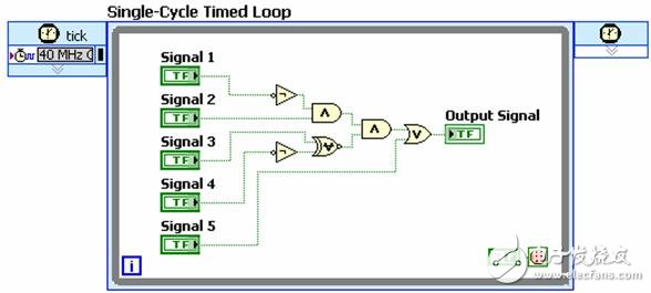
Figure 9. Simple Boolean Logic with STCL
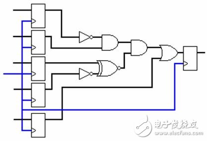
Figure 10. Corresponding circuit diagram of Boolean logic shown in Figure 9.
Obviously, this implementation is much simpler. In Virtex-II or Spartan-3 series FPGAs, the logic between flip-flops requires at least two 4-input lookup tables, as shown in Figure 11.
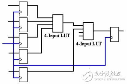
Figure 11. Dual four-input lookup table implementation of the circuit diagram in Figure 10.
Since the Virtex-5 family of FPGAs has a 6-input lookup table, users can implement the same amount of logic in a lookup table, as shown in Figure 12.
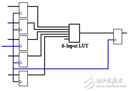
Figure 12. Double six input lookup table in Figure 10.
The SCTL used in this example (shown in Figure 9) is set to run at 40 MHz, which means that the logic must be executed within 25 ns between any flip-flops. The speed at which electrons travel in a circuit determines the maximum speed at which the code executes. The key route is the branch of the logic circuit with the longest propagation delay, which determines the theoretical maximum clock rate in that part of the circuit. The dual six-input lookup table on the Virtex-5 FPGA not only reduces the total number of lookup tables required to implement a given logic circuit, but also reduces the propagation delay (time) of electrons through the logic. The 6-input lookup table in the Virtex-5 family of FPGAs not only reduces the number of lookup tables needed to implement a particular logic, but also reduces the propagation delay of current in the logic. This means that you can set a faster time speed simply by choosing a Virtex-5 based hardware metric to set the same SCTL.
Check out the list of countermeasures in the white paper below for more information on Virtex-5 FPGAs.
5. Multiplier and DSP chip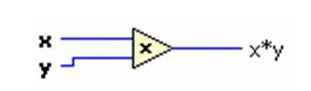
Figure 13. Multiplier function
The seemingly simple two-digit multiplication operation is very complicated to implement in digital circuits and is extremely resource intensive. To provide a related reference, FIG. 14 is a schematic diagram of implementing a 4&TImes; 4-byte multiplier using a combinational logic circuit.
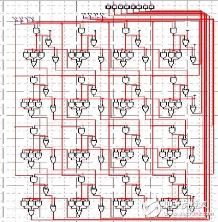
Figure 14. Circuit diagram of multiplication of two 4-byte inputs
Imagine multiplying two 32-byte numbers to get results by more than 2000 steps. Therefore, the FPGA presets the multiplier circuit and saves it for lookup tables and triggers in math and signal processing applications. Virtex-II and Spartan-3 FPGAs have 18&TImes; 18-bit multipliers, so the operation of multiplying two 32-byte numbers requires three multipliers. Many signal processing algorithms include the ability to multiply results. Therefore, high-performance FPGAs such as Virtex-5 preset a multiplier accumulator circuit called a DSP chip. These preset processing components, also known as DSP48 slices, include 25&TImes; 18-bit multiplier and adder circuit, although you can use the multiplier function alone. Table 5 shows the DSP decisions for different FPGA families.
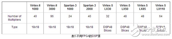
Table 5. DSP Sources for Different FPGAs
6. Block Random Access Memory (RAM)When choosing an FPGA, the memory source is another key factor to consider. User-defined random access memory (RAM) embedded in the FPGA chip is useful for storing data settings or transferring values ​​between parallel loops. Based on the FPGA family, you can set onboard RAM in 16 or 36kb components, or use flip-flops to perform data setup in arrays; however, for FPGA logic sources, large arrays quickly become "luxury." More than 30% of the triggers in the Virtex-II 1000 FPGA can be consumed by 100 32-byte element arrays, or less than 1% of the embedded block RAM. DSP algorithms typically need to track the entire block of data or the coefficients of a complex equation, and in the absence of onboard memory, many of the processing functions are not available in the hardware logic of the FPGA chip. Figure 16 shows the graphical function of reading and writing memory using block RAM.
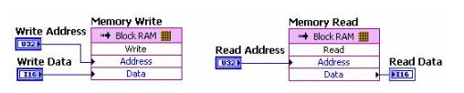
Figure 15. Block RAM function for reading and writing memory
Similarly, you can use memory blocks to store a complete cycle as a sequence of values ​​and indexes, storing periodic waveform data for the onboard signal generator. The final frequency of the output signal is determined by the speed at which the value is retrieved, so that you can use this method to dynamically change the output frequency without the need for sharp changes in the input waveform.
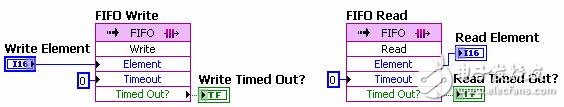
Figure 17. Block RAM function for FIFO buffer
The inherent parallelism of FPGAs requires logic circuit independent components to be driven without time pulses. Passing data between logic circuits at different operating speeds is tricky. When using a first in first out (FIFO) buffer, the onboard memory can be used to make the transmission smoother. As shown in Figure 16, the user can configure the FIFO buffers to different sizes to ensure that data is not lost between the asynchronous components of the FPGA chip. Table 6 shows the user-settable fast RAM embedded in different FPGA families.
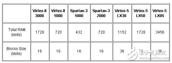
Table 6. Memory Sources for Different FPGAs
7. SummaryWith the development of high-end technology and the in-depth summary of new concepts, the adoption of FPGA technology will continue to increase. However, exploring the mysteries of FPGAs, it is also very important to sigh the changes compiled in the block diagrams in this silicon chip. In the development phase, if you know how to utilize and optimize resources, it is helpful to compare and select hardware metrics such as triggers, lookup tables, multipliers, and block RAM. These basic functional blocks are not a complete list of all resources, and this white paper does not contain a discussion of all FPGA components. Users can continue to learn about FPGA and digital hardware design with the recommended resources below.
Board-To-Board Connectors,Machine-Pin Board-To-Board Connectors,Gold Plated Board-To-Board Connectors,8 Pin Board-To-Board Connectors
Shenzhen Jinyicheng Electronci Technology Co.,Ltd. , https://www.jycconnector.com