Design and Implementation of a Multi-channel Data Acquisition System Based on FPGA
Abstract: Based on the characteristics of PCI bus and FPGA, a multi-channel signal acquisition and transmission system with high precision, high stability and high accuracy is designed. The system adopts FPGA as the main control unit, and controls the analog signal acquisition by controlling the analog selection switch ADG706 and the A/D converter AD7667, and the collected data is uploaded to the upper computer for analysis by the FIFO buffer through the PCI bus. Through practical application, the system performance is stable and meets the design requirements.
Data acquisition is to adjust the parameters (physical quantity, chemical quantity, biomass, etc.) of the object to be tested (physical quantity, chemical quantity, biomass, etc.) through various sensing elements, and then adjust, sample, quantize, encode, and transmit. Finally, it is sent to the controller for data processing or storage recording process [1]. Data acquisition techniques can digitize many abstract analog quantities, give them their magnitude, or analyze the analog quantities through signal processing. Based on the high clock frequency, small internal delay, simple and precise timing control, and flexible programming configuration of the FPGA device, the system uses FPGA as the core to control channel switching analog-to-digital, conversion, data frame and transmission. In addition, based on the advantages of high stability of PCI bus, fast data transmission and strong expansion, the PCI bus is used to realize the seamless connection between the host computer and the FPGA, and the data transmission between the host computer and the FPGA control module is completed.
1 system design 1. 1 system compositionThe system collects 29 high-frequency pressure signals (including a speed-changing signal with a 4-channel sampling rate of 40 K and a slowly-changing signal with a 25-channel sampling rate of 6. 6 K). The design is modular in design. The entire system is integrated and independent of each module. The system is mainly composed of a signal acquisition module, an FPGA control module, a PCI bus interface module, and a power module. The modular design facilitates circuit debugging, programming and expansion, as well as the ability to quickly locate and solve problems quickly. In this system, considering that the control program occupies more logic resources, the FPGA control module uses Xilinx spartan-3 series chip XC3S400 as the main control chip to connect with peripheral devices. The overall block diagram of the system is shown in Figure 1.
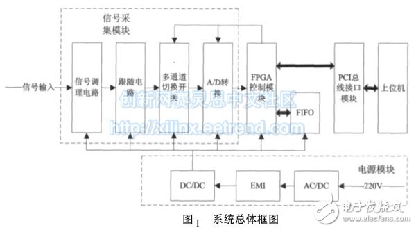
The system is powered on and then acquires and transmits functions without waiting for the command word. The analog signal is amplified by the op amp OPA4340, and then enters the first-order filter circuit and the voltage follower for signal conditioning. Then, under the timing control of the FPGA, the strobe of the analog selection switch ADG706 enters the AD7667 for analog-to-digital conversion, and the converted data buffer In the FIFO, it is finally uploaded to the host computer for display and analysis via the PCI bus interface circuit. The power supply of the whole system is provided by the power module. The power module has its own EMI module for filtering protection, and supplies the required 5 V, 3.3 V and 1.2 V voltages to the FPGA control module to provide the required 5 to the signal acquisition module. V, 3. 3 V voltage.
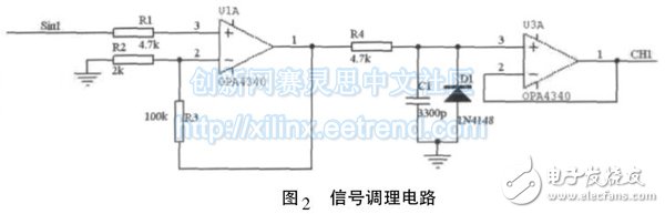
2 hardware circuit design 2. 1 signal conditioning and follower circuitAfter the high-frequency pressure signal enters the system, the signal conditioning circuit is first used to complete the amplification, filtering, and follow-up of the signal. The conditioning circuit is shown in Figure 2. After the signal amplification circuit, the signal amplitude is adjusted to the range of 0-5 V. Afterwards, the first-order filter circuit is passed, wherein the filter circuit cut-off frequency is, so that the frequency range of the input signal is adjusted into the frequency range of the system acquisition signal, and finally enters the analog switch ADG706. D1 in Figure 2 acts as a reverse protection.
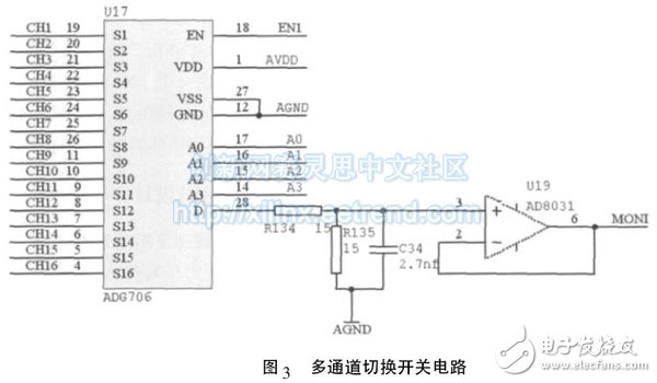
The 16-channel analog switch ADG706 converts the analog signals to the analog-to-digital converter AD7667 for A/D conversion. Two ADG706s can be used to switch between 29 analog signals. FPGA control module for analog switch during design
The ADG706's enable control and channel switching control are issues that should be noted in the design. In addition, the signal will enter the voltage follower after passing the ADG706. The high-speed op amp AD8031 selected by the follower here knows that the maximum capacitive load is 15PF according to the chip data, which is much higher than the driving capability of the AD8031. Therefore, it is possible to cause an oscillation problem. The addition of a first-order active filter circuit in the design can filter out high-frequency oscillations. The multi-channel switch circuit is shown in Figure 3.
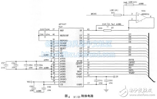
The AD7667 analog-to-digital converter in this system has a sampling capability of 16 bit / 1 M. After the input signal is converted into a 16-bit digital signal, the upper 8 bits and the lower 8 bits are sequentially taken under the control of the FPGA, and sequentially written into the FIFO buffer according to the designed frame structure. In the design, the analog signal is conditioned and regulated in the range of 0 to 5 V before entering the AD7667. Since the AD7667 has a 2. 5 V reference voltage source, the signal before the AD7667 is divided by the resistor network. The voltage range after the voltage divider is:
(0 to 5 V) &TImes; 10 K/( 12 K +10 K) = (0 to 2.25 V).
The result is within the voltage input range of the AD7667. In addition, C49 is a decoupling capacitor, which is used to reduce the interference caused by power supply, noise and so on. The A\ \D conversion circuit is shown in Figure 4.
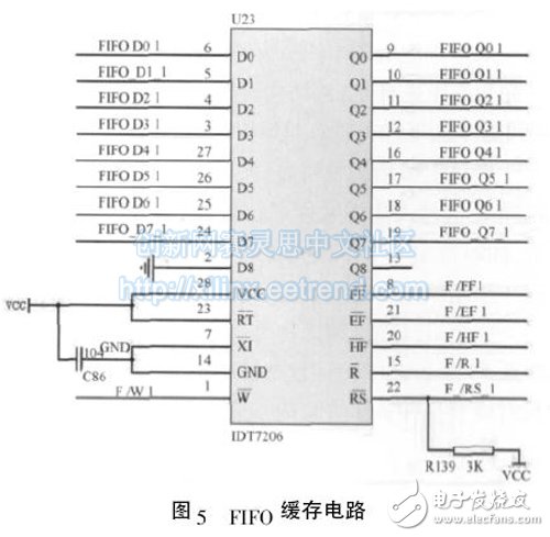
This system uses the external FIFO IDT7206. This is because the external FIFO pin has many functions, especially the half full signal and the null signal are easy to judge, and it does not occupy the internal resources of the FPGA. In this design, the IDT7206 adopts a half-full-read mode of operation, so that FIFO buffer data overflow does not occur, and the cached data can be read out at high speed to achieve the purpose of caching. The FIFO buffer circuit is shown in Figure 5.
PCI bus interface module adopts PCI904 PCI bus universal interface chip PCI9054, PCI9054 conforms to PCI V2.1 and V2. 2 specifications, has two independent programmable DMA controllers, data width 32 bits, theoretical data transmission rate up to 132 MBps [2]. In order to meet the high-speed transmission between the host computer and the PCI bus module, the PCI9054 adopts the DMA burst transfer mode.
When the FPGA control module detects that the “half full†signal of the FIFO is low, the data in the FIFO is read out to form a specified data packet, and the PCI9054 is controlled to transmit data to the upper computer.
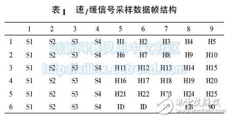
3 system timing design 3. 1 signal sampling frame structure design Sampling the frame structure, ie the signal sampling order (channel switching order), is the most important part of the design. In the case of guaranteeing the sampling rate of each signal, it is a key point of design to average the sampling time intervals of the same signal in one frame structure. The parameters of the fast/slow-change analog signal to be sampled in this system are as follows:
S: is a fast change signal, 4 channels (S1 ~ S4), sampling rate: 40Ksps, 8 bit;
H: is a slowly changing signal, 25 channels (H1 ~ H25), sampling rate: 6. 6Ksps, 8 bit;
The fast-changing signal sampling rate is 6 times that of the slow-changing signal sampling rate, so there is no need to increase the overall sampling rate of the system. First, determine the number of rows of the frame structure: Place the S with a high sampling rate at the beginning of the frame structure. Since the sampling rate is 6 times that of 6.6 Ksps, the sampling point of the S signal in one frame should be the H signal. 6 times, it is determined that one column of the frame structure is 6 sampling points, the number of rows of the frame structure is 6, and the first 4 columns of the frame structure are sampling points of S, so the number of frame structure columns should be greater than 4.
Then determine the number of columns of the frame structure: Since one column is 6 sample points, the H signal occupies 25 samples, which requires 5 columns to be put down, and 5 vacancies are just used to place the frame count and frame mark. The number of columns in the frame structure is then: 4 + 5 = 9.
It can then be determined that the frame structure is a matrix of 6 &TImes; 9 with a total of 54 sampling points. The frame count and frame mark occupy 5 sample points, and we get a sample frame structure as shown in Table 1.
The strobe of the analog switch in this system, the control of A \ \D, the read and write of the FIFO are controlled by the FPGA, and the total sampling rate of the signal is
6. 6 K &TImes; 54 = 360 Ksps. The FPGA's clock frequency is 54MHz, so the FPGA internal logic has 150 state machines available at each sample point, which is sufficient for analog switch channel switching, A\ \D analog-to-digital conversion, and FIFO buffering. In addition, the analog switch switching and starting A \ \D conversion are separated as much as possible. This arrangement is mainly for the analog signal to have enough time to stabilize before the channel switching, so as to improve the sampling accuracy [3]. The FPGA control timing diagram is shown in Figure 6 below.
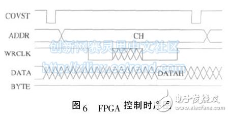
In Figure 6: COVST is the AD sampling control signal, active low; ADDR is the analog switch switching address of the output; WRCLK is the FIFO write signal, the rising edge is valid; DATA is the data to be written into the FIFO; BYTE is the byte output The control signal takes the lower 8 bits of the data when low, and the upper 8 bits of the data when high.
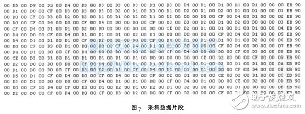
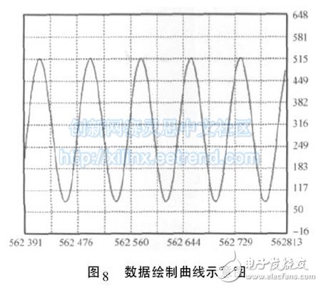
4 test results analysisIn practical applications, the collected data is uploaded to the host computer through the PCI bus, and a part of the uploaded data is shown in FIG. 7 . It can be seen from Fig. 7 that the format of the uploaded data frame is complete, the frame marks are aligned, the frame count is correct, and there is no number loss phenomenon. The curve drawn by the data processed by the host computer is shown in Figure 8. The signal input is a sine wave. It can be seen from Figure 8 that the system sampling function is normal and the waveform is complete. In summary, the system is fully functional and the performance meets the design requirements.
This design is designed for the acquisition and transmission technology requirements and current technical implementation methods. It has completed the design of multi-channel signal acquisition and transmission system, organically combined FPGA and PCI bus technology, making full use of their respective advantages, enabling the acquisition system to have real-time acquisition and real-time. The functions of display, instant feedback, automatic processing and automatic transmission provide reliable guarantee for the authenticity, validity, real-time and availability of data collected in the field.
The USB 3.2 specification absorbed all prior 3.x specifications. USB 3.2 identifies three transfer rates – 20Gbps, 10Gbps, and 5Gbps.
Key characteristics of the USB 3.2 specification include:
Defines multi-lane operation for new USB 3.2 hosts and devices, allowing for up to two lanes of 10Gbps operation to realize a 20Gbps data transfer rate, without sacrificing cable length
Delivers compelling performance boosts to meet requirements for demanding USB storage, display, and docking applications
Continued use of existing USB physical layer data rates and encoding techniques
Minor update to hub specification to address increased performance and assure seamless transitions between single and two-lane operation
Improved data encoding for more efficient data transfer leading to higher through-put and improved I/O power efficiency
Backwards compatible with all existing USB products; will operate at lowest common speed capability
Usb 3.2 Cable,Usb Type-C Cable,5Gbps Usb Type-C Cable,10Gbps Usb Type-C Cable
UCOAX , https://www.ucoax.com