FPGA engineering implementation of multi-beamforming in imaging sonar
Abstract: This paper proposes a high-speed FPGA implementation method with near-field focusing multi-beam formation with simple calculation method, small calculation amount and small required storage. It is used for multi-beam with high precision, high coverage and high beam number in imaging sonar. form. The method is based on a 180-element uniform semi-circular array. By rotating the equivalent chord of the array element, only 540 beams can be generated in the 90° range by using 6 sets of weighting coefficient vectors, so that the storage amount is reduced by two orders of magnitude, thereby effectively reducing Requirements for hardware storage resources. The system works at 270MHz, and realizes uninterrupted input and output of data through ping-pong operation, thereby improving speed. Through multi-channel multi-coefficient multiplier and parallelism of pipeline, only 540 beams are generated in real time by using 24 multipliers. 8190 times reuse is achieved. Compared with the traditional parallel processing architecture, this method improves system stability and speed, and greatly saves FPGA hardware resources.
Introduction Because the imaging system has many channels, large amount of data, complicated calculation, and real-time imaging characteristics [1][2], it requires the processor to have high speed, high precision, large storage capacity and the premise of ensuring the sensitivity of sonar. The ability to process in real time [3]. Compared with other CPUs and DSP processors, FPGAs have unmatched system-level user-programmable features and powerful parallel computing capabilities for high-speed, high-density high-end digital logic circuit designs. In addition, FPGAs have very high performance I/O bandwidth. A large number of I/O pins and multiple blocks of memory allow the system to achieve superior parallel processing performance in designs for imaging sonar systems with 180 channel signal inputs. Real-time signal processing of imaging sonar can be realized by using FPGA [4-6].
Because of the large amount of beam weighting data that needs to be stored in the FPGA, the amount of block RAM inside the chip is an important factor in selecting the chip. Weigh the speed of the work and the various resources and costs of the chip itself, and choose the vc6vlx130t of the Virtex-6 series to implement the system.
Imaging sonar often works in the near field. In the near-field range, the acoustic wave is approximated as a spherical wave. The directivity is a function of distance, so it must be corrected by near-field focusing [7-11]. In this paper, the method of focusing all beams is used to calculate the compensation phase focused at different distances in advance and store them in the memory for calling during beamforming.
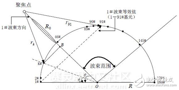
Figure 1 Schematic diagram of multi-beam formation in near-field aggregation
According to the needs of the system, there may be more than one focal plane position. The position of the focal plane does not affect the operation speed, but only consumes a little more ROM resources. In order to reduce storage requirements, the number of focal planes should be reduced as much as possible without degrading performance. In this paper, beamforming can be performed in the near-field (r<18m) range by allowing 7 focal planes with a 0.001° error in the main lobe direction, a sidelobe level of less than -14 dB, and a main lobe width of no more than 1°. The focusing distance is from 1 meter to 18 meters (within 1 meter as a blind spot, regardless of), the distance between the focal planes is not uniform, but increases as the distance of the sound source increases.
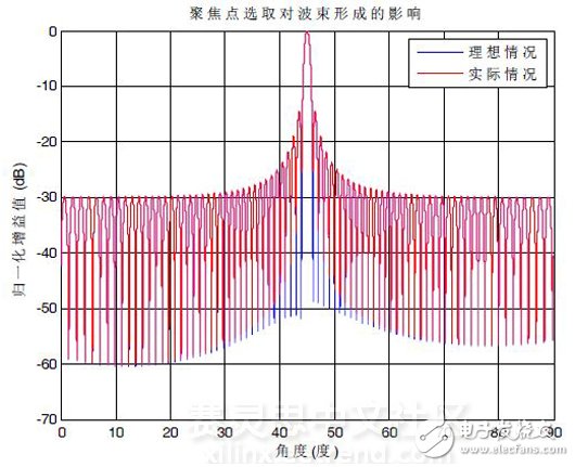
Figure 2 1# beam pattern of aggregate beamforming
The position of the target is centered, and the position of the target is represented by (distance, orientation). Assuming that the sound source is located at (1m, 45°), the effect of different focal planes on beamforming is shown in Figure 5. The blue line is ideally used, focusing at the same focal length (1.1m) as the actual location. The 1# beam pattern has a beam pointing at 45°, a main lobe width of 0.9010°, and a sidelobe level of -14.47 dB. When the red line is the actual working condition of the sonar system, the approximate distance is selected according to the above-mentioned eight focusing faces, and the 1# beam pattern when focusing at 1.05 m is adopted. The beam pattern in both cases agrees well. Therefore, although only 7 focal planes are used for near-field beamforming, the effect on beamforming is not significant, but the utilization efficiency of system resources can be greatly improved.
2 FPGA implementation of multi-beamformingBecause digital multi-beamforming needs to process a large amount of data, and has high processing speed requirements, but the computing structure is relatively simple, it is suitable for multi-channel parallel processing using FPGA, while taking into account speed and flexibility.
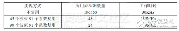
Digital multi-beamforming (DBF) mainly performs complex multiplication and complex addition, and each input signal is a baseband I/Q component that is output after down-conversion. A single-beam DBF with 91 array elements is required to complete 364 multiplications and 363 addition operations of real numbers, and the main factor affecting computation speed and resource consumption in the FPGA is the multiplier. If only parallel processing is used, generating 540 beams requires 540&TImes; 91 & TImes; 4 = 196560 multipliers, which consume a large amount of multiplier resources and cannot be implemented on one FPGA. On the other hand, the single-channel data input beamformer has a speed of 30KHz, and the FPGA's chip processing speed can usually reach several hundred megabytes, so you can take advantage of the high-speed performance of the FPGA, make full use of the multiplier resources, and pass the time division multiplexing multiplier ( TDM) implements multi-channel data multi-coefficient multiplication. Using 90 beams and 91 coefficients to share a multiplier, 8190 times multiplexing is achieved, and the number of multipliers required to generate 540 beams is reduced to 24, as shown in Table 1.
Table 1 Relationship between resource utilization and speed
Digital multi-beamforming is divided into six modules, each of which uses the same set of weighting coefficients to produce 90 beams, as shown in Figure 3:
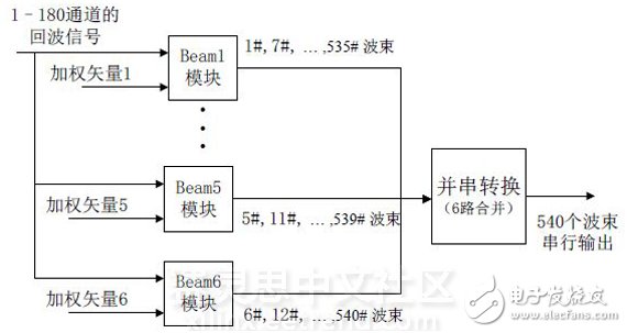
Figure 3 DBF overall functional block diagram
The Beam1-beam6 module has the same function. The only difference is that the input weight vector data is different. Therefore, the beam1 module is taken as an example to illustrate its FPGA implementation process. The FPGA-based multi-beamformer is implemented by several parts such as memory module, control module and multiply-accumulate module. The block diagram of the system is shown in Figure 4.
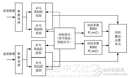
Figure 4 Beamforming FPGA implementation function module
2.1 The data processed by the front end of the storage module uses ping-pong operation to achieve uninterrupted data writing and output. The real data and imaginary data are stored in separate dual-port RAM, as shown in Figure 4, the real RAM1 and the imaginary RAM2. Since the data to be buffered is 16 bits of data on 180 channels, the capacity of the ping-pong RAM should be twice that of the buffered data, ie 16 & TImes; 180 & TImes; 2 × 2 = 11.25 Kbit.
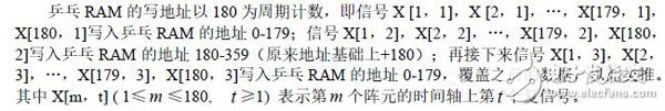
The reading order of the ping-pong RAM is special: in order to accelerate and save the multiplier resources, the real multipliers are used to realize the multiplexing of 91 coefficients of 90 beams, so the read clock is 90×91/180=45.5 times of the write clock. The reading sequence is as follows: reading the signal data of the 0-99 address unit for generating the 1# beam, then reading the signal data of the 1-100 address unit for generating the 7# beam, ..., reading the signal of the 88-187 address unit The data is used to generate the 529# beam, and finally the signal data of the 89-188 address unit is read for generating the 535# beam. After reading the data, the signal data of the next moment has been written into the 180-359 address unit. At this time, after adding 180 to the above read address, the read data is used to generate 540 beam data at the next moment, in turn. Cycle back and forth.
The on-chip ROM stores beam weighting coefficient vectors, and the six beamforming modules use respective coefficient ROMs. The read clock is the same as the ping-pong RAM, and the read address is relatively simple, repeating the address 0-90, and determining which weighting coefficient vector of the focus plane is called according to the data point position.
2.2 The control module control module generates read and write address signals and control signals, and controls the read and write addresses of the ping-pong RAM and the coefficient ROM according to the above contents; the control signal portion mainly generates the operation of the control operation portion and the storage portion. control signal.
2.3 The arithmetic module signal data and the corresponding weighted data are read out and serially entered into the multiply-accumulate module at a rate of 270M. The complex multiplication is one of the most important operations. Assume that the signal of the receiving channel is expressed as:
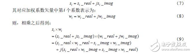
First, the 1-91 channel data serially enters the multiply accumulator, and after 91 complex multiplications and 90 complex additions, a beam data containing the real part and the imaginary part is obtained; after that, the 2-92 channel data enters the multiplication accumulation. The second beam data is obtained. Thus, 90 beams are formed, and only one complex multiplier, that is, four real multipliers is required.
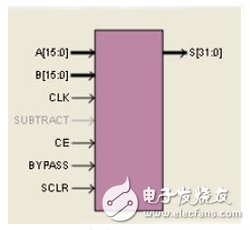
Figure 5 Multiply Accumulator IP Core
The multiplication and multiplication is implemented by Xilinx's IP core, as shown in Figure 5. The meaning of each parameter is shown in Table 2.
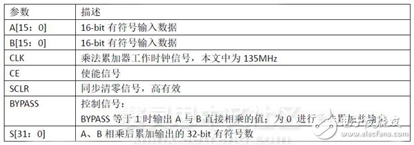
Table 2 Multiplication and accumulation of IP core parameters meaning
The multiplication accumulating process is controlled by controlling the BYPASS signal: when the filtered data and the weighting coefficient are valid, BYPASS is maintained at a high level for one period and then becomes a low level, and after counting for 100 cycles, it becomes a high level again, and the next one is started. The beam data is calculated, so the bypass period is 1.35 MHz.
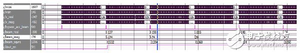
Figure 6 Beamforming module waveform
As shown in Figure 6, the beam data output rate is 2.7MHz, corresponding to a single beam output rate of 30KHz, and the calculation results are consistent with the MATLAB simulation results. After the real and imaginary parts of each beam are output, the square of the beam is obtained by multiplication.
3 verification resultsThe signal is directed from the 90° direction of the array to the primitive, and the 1# primitive to the 180# primitive receives the signal, and the signal at each primitive is obtained by the delay of the primitive and the beam point. The signals of 180 primitives are collected simultaneously, and 4 points are collected in one cycle, and the collected data is used as a standard signal source. When the system is designed, the standard signal source data is stored in the signal processing unit. During the operation of the system, if the signal processing unit receives a command using a standard signal source, the standard signal source data is read out for filtering extraction and multi-beam forming operation. Compare the beam output of the system with the MATLAB simulation results to check if the system is working properly.
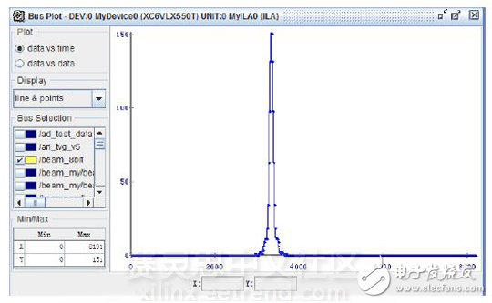
Figure 7 Chipscope verification standard signal source test
Figure 7 shows the beam values ​​of 540 beams at a certain time when Chipcsope is used to test with a standard signal source, which has good directivity.
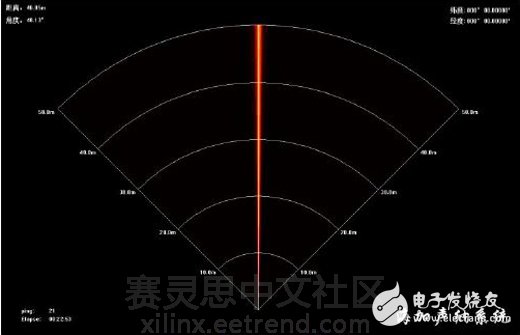
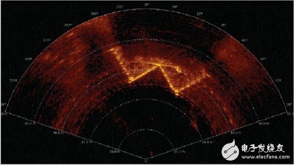
Figure 8 standard signal source test image
Figure 8 shows the display image obtained by the actual system using the standard signal source test and transmitting the beam data to the PC through the Gigabit network, which is a bright stripe in the 90° direction.
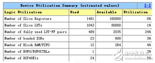
Figure 9 FPGA resource utilization
The improved algorithm proposed in this paper only needs 6 sets of weighting coefficient vectors to generate 540 beams, which effectively reduces the requirements for storage resources. Through ping-pong operation, uninterrupted data input and output, as well as parallel processing of pipelines, enable real-time processing. The multi-channel multi-coefficient multiplexing technology reduces the multiplier resource usage to 24, which greatly saves the FPGA hardware resources. The FPGA resources used for digital multibeamforming are shown in Figure 9, which uses only a small portion of the entire chip resources, providing ample room for the implementation of the rest of the imaging sonar system.
Conclusion This paper proposes a multi-beam forming method that implements high-speed multi-channel using FPGA. Through ping-pong operation and parallel processing of pipelines to improve speed; through multi-channel multi-coefficient multiplexing multiplier and module multiplexing technology, only 540 beams of 180 channels of data are generated in real time by using 24 multipliers, which effectively reduces the utilization of FPGA resources. Suitable for implementing multi-beam forming systems on engineering.
Digital Signage Player,Electronic Signage,Signage For Hotels,Commercial Digital Signage Displays
Guangdong Elieken Electronic Technology Co.,Ltd. , https://www.elieken.com