Design of Voice Signal Compression Storage System Based on TMS320C5402
1 Voice signal compression principle μ/A law compression and decompression coding is the first G.711 voice compression decompression coding introduced by the CCITT (Consultative Committee for International Telegraph and Telephone). Among them, countries such as Europe and China adopt A-law compression and decompression coding, and countries such as the United States and Japan use μ-law compression decompression coding. Since the system uses the A-law compression and decompression algorithm, only the A-law compression principle is introduced here.
The mathematical analytical formula of A-law companding is:
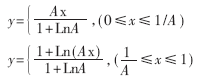
Where: y is the output signal; x is the input signal; A is the compression factor.
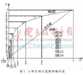
It is known from the above equation that the small signal is linear and the large signal is approximately logarithmic. This companding feature often combines compression, quantization, and coding. The A law can be approximated by a 13-segment polyline (equivalent to A=87.6), which is easy to implement with digital circuits [1]. The compression characteristics of the 13-segment line are shown in Figure 1. The segment of Fig. 1 is the case when x takes a positive value, and when x takes a negative value, the companding property is oddly symmetric with the positive value of x. In the positive 8 segment and the negative 8 segment, positive 1, 2 segment and negative 1 The slopes of the two segments are the same and are combined into one segment, so the original 16-segment polyline becomes a 13-segment polyline.
This article refers to the address: http://
When performing A-law compression, the sampled 12-bit data defaults to the highest-order sign bit. When compressing, the highest bit, that is, the sign bit is kept unchanged, and the last 11 bits of the original data are compressed to 7 bits. This 7-bit code consists of a 3-bit paragraph code and a 4-bit segment inner code. The compressed transformed data is determined based on the size of the last 11 bits of data. The specific coding table is shown in Table 1.

2 system hardware interface design The system implements the G.711 standard A-law compression coding speech processing process. The system uses TMS320C5402 as the core to complete the voice compression, storage and decompression functions. The voice acquisition and output module uses TI's high-performance stereo audio Codec chip TLC320AD50C with built-in input and output amplifiers and programmable gain adjustment for both input and output.
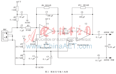
2.1 Analog Interface Design The analog signal input circuit is shown in Figure 2. The speech signal amplifier is amplified by a front-end amplifier TLC2272ACD, bandpass filtered, and the single-input signal is converted to a differential signal and sent to the differential inputs (INP and INM) of the A/D converter of the AD50C. The A/D converter converts the input analog signal into a digital signal expressed in two's complement.
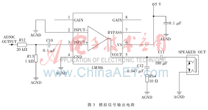
The analog signal output circuit is shown in Figure 3. The analog signal recovered by D/A conversion and internal low-pass filtering is output from the OUTP pin of the AD50C. The external amplification filter circuit uses the LM356 operational amplifier, and the amplified signal is sent to the speaker to restore the sound.
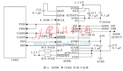
2.2 Digital Interface Design The TLC320AD50C supports seamless interfacing with the TMS320C5402. The interface circuit is shown in Figure 4. Set the TLC320AD50C to active mode, the input master clock MCLK is 8.192 MHz, the sampling frequency is selected to be 8 kHz, and the internal PLL is enabled (N=8 in Control Register 4) [2]. The FSX, FSR, CLKR, and CLKX of the TMS320C5402 are configured as external inputs through register settings, and the SCLK of the TLC320AD50C is internally generated. The data receiving/transmitting frame synchronization signal and the shift clock signal are all generated by the TLC320AD50C, and the receiving/transmitting process of the serial port is controlled by the TLC320AD50C.
3 system software interface design system program flow chart shown in Figure 5, software design work mainly includes the following aspects:

(1) Initialization of the TMS320VC5402 serial port. First reset the DSP serial port 0, and then program the serial port 0 register, so that the DSP serial port works in the following state: run in SPI mode, one phase per frame, one word per phase, 16 bits per word, frame synchronization pulse low level Valid, and the frame sync signal and the shift clock signal are generated externally [3].
(2) AD50C initialization. The initialization process includes sending 2 strings of 16-bit digital information to the AD50C through the synchronous serial port of the TMS320C5402. The first string is 0000 0000 0000 0001B, and the least significant bit (bits0) is 1, indicating that the next data word to be transmitted belongs to the secondary communication. The second data is used to configure one of the four control registers of the AD50C. The 15~11 bits are 0, the 10~8 bits are the selected register address values, and the 7~0 bits are the programmed values ​​of the selected registers. By programming the four programmable control registers, the AD50C operates in the following states: select INP/INM as the active analog input, 15+1 bit ADC and 15+1 bit DAC mode, without slave, sampling frequency is 8 kHz, The analog signal input and output amplification gains are both 0 dB [4]. Four register initializations require four primary and secondary communications.
(3) Implementation of the companding algorithm. The buffered serial port (McBSPs) inside the TMS320C5402 is equipped with hardware-implemented μ-law and A-law compression decompression. The user only needs to set it in the corresponding register. The system converts the linear code into A law through software programming. In the main program, the linear coding is obtained by A/D sampling quantization, and then the 8-bit A-law coding is obtained by software calculation. The highest bit is the sign bit, the sixth bit to the fourth bit are the paragraph code, and the lower 4 bit is Intra-segment code. The 8-bit compression result is stored in the system RAM for buffering, and the size of the voice storage buffer is set according to the sampling rate, the voice storage time, and the system RAM capacity. After the buffer is full, the data in the buffer is decompressed. And then output to the SPEAKER interface output.
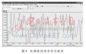
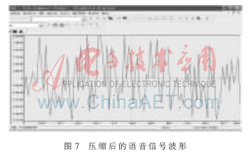
4 System experiment results After the hardware debugging is successful, the recording time is about 5 s. The data pattern is observed by CCS. Figure 6 shows the waveform of the voice signal before compression, and Figure 7 shows the waveform of the voice signal after compression. After playback, the voice signal has no obvious distortion after audition. The experimental results show that the system successfully implements the compressed storage of voice signals.
The MS320C5402 and TLC320AD50C components of the speech compression storage system described in this paper are simple, easy to program, and the program code has been verified in the CCS3.1 development environment.
references
[1] Song Yiqing, He Song. A New Method Based on Linear and Nonlinear Quantization Conversion of DSP Speech Signals[J].Microelectronics & Computer,2008(11):36-39.
[2] Xu Su. Real-time voice compression based on DSP[J]. Microcomputer Information, 2007(2): 61-64.
[3] Li Li. DSP principle and practical application technology [M]. Beijing: China Water Resources and Hydropower Press, 2004: 200-210.
[4] TLC320ADC/TLC320AD52C Data Manual. Texas Instruments, 2002.
60V20Ah Lithium Ion Battery,Waterproof Battery Pack For Bicycle,60V 20Ah L-Ion Waterproof Battery,Rechargeable 60V Lifepo4 Lithium Battery
Jiangsu Zhitai New Energy Technology Co.,Ltd , https://www.ztbatteries.com