Future prospects of diamond-based gallium nitride (GaN) technology
In the past ten years, the research boom of gallium nitride (GaN) has swept the global electronics industry. This kind of material is a wide-bandgap semiconductor material. It has excellent performance such as large forbidden band width, high thermal conductivity, high electron saturation drift speed, and easy formation of heterostructures. It is very suitable for the development of high-frequency, high-power microwaves, millimeter waves, etc. Devices and circuits are the most ideal semiconductor materials for developing microwave power devices in the past 20 years. With the continuous improvement of the crystal quality of epitaxial materials and the continuous improvement of device technology, microwave and millimeter wave devices and circuits developed based on GaN-based materials have higher and higher operating frequencies and higher output power.
With the development of microwave power devices based on gallium nitride (GaN) materials in the direction of smaller size, larger output power and higher frequencies, the problem of "heat" has become more and more prominent, and has gradually become a constraint on this kind of devices. One of the most important issues for performance improvement. Using high thermal conductivity diamond as the substrate or heat sink for high frequency and high power gallium nitride (GaN) based devices can reduce the self-heating effect of gallium nitride (GaN) based high power devices and is expected to solve the increase in total power The problem of rapid decline in power density due to frequency increase has become an international research hotspot in recent years.
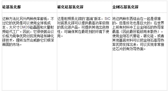
Comparison of silicon, silicon carbide (SiC), and diamond-based GaN
Diamond-based gallium nitride (GaN) technology
Diamond has the highest thermal conductivity among the currently known natural substances. The thermal conductivity at room temperature is as high as 2000Wm-1K-1, which is four to five times that of silicon carbide. As a substrate material, diamond can be deposited in the GaN channel with a size of hundreds of nanometers, so that the transistor device can effectively dissipate heat during operation. It has great application potential in the heat dissipation of high-frequency, high-power GaN-based high electron mobility transistors (HEMT) and circuits.
Felix Ejeckam invented GaN on diamond in 2003 to effectively extract heat from the hottest location in a GaN transistor. The basic idea is to use colder GaN amplifiers to make the system more energy efficient and reduce waste. The GaN wafer on diamond is stripped from the original Si substrate through a GaN channel or epitaxy, and then bonded to the CVD synthetic diamond substrate through a 35 nm SiN interface layer. This kind of 200°C GaN channel and CVD to form nanoscale diamond is close to the most thermally conductive industrial material, it will greatly reduce the temperature rise between the amplifier substrate and the channel. Figure 1 shows the manufacturing process of GaN on a diamond wafer. Over the years, many research groups have quantified the aforementioned thermal improvement. First, the Si-based GaN HEMT wafer is pasted on a temporary Si carrier. After the original silicon substrate is etched away, the CVD method is used to deposit diamond on the 35 nm interface layer below the GaN layer. Finally, the temporary Si carrier is etched, and the final GaN wafer on diamond is processed into HEMTs or MMICs.
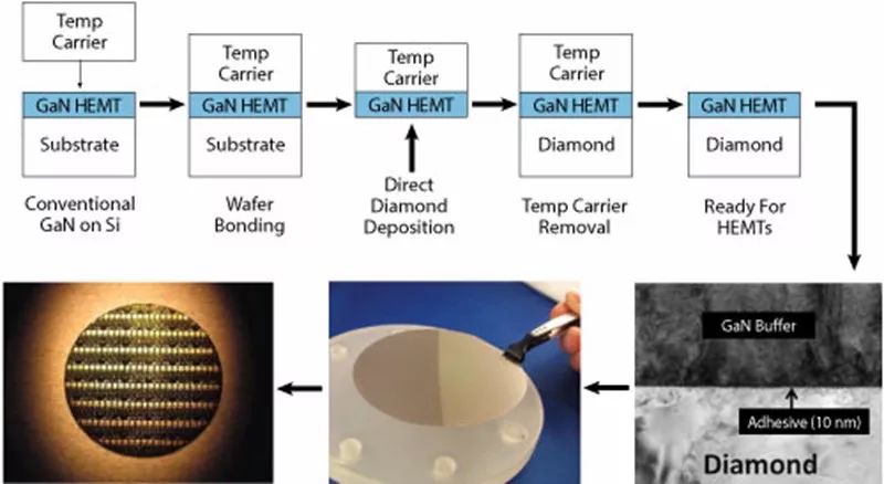
Figure 1 The production process of GaN on diamond wafers
Technical system impact
Compared with GaN on SiC, if the heat generated by GaN MMIC can be reduced by 40% to 50%, then greater power density can be compressed into a smaller volume space. Power is a direct parameter for calculating the downlink data rate. The higher the power, the more information is transmitted. In a very compact space, the use of GaN on diamond can reduce the requirements for the cooling system. Because compared with the use of standard SiC-based GaN power amplifiers, the use of GaN on diamond allows the ambient temperature to rise higher without reducing performance and reliability. The reduction of cooling devices also means a reduction in weight and size.
The inventor of diamond-based gallium nitride establishes Akash Systems
In 2003, Ejeckam, who also worked at Group4 Lab, invented diamond-based gallium nitride by transferring a GaN epitaxial layer grown on silicon to a synthetic chemical vapor deposition diamond substrate. The assets of Group4Lab were acquired by ElemenSix Technology Company, one of the De Beers Group member companies in 2013. Felix Ejeckam and TyMitchell jointly established Akash Systems in San Francisco, California, USA in 2016, and reached an agreement with South Korea's RFHIC to jointly negotiate and buy back the diamond-based gallium nitride patent.
Diamond-based GaN application: satellite communication power amplifier
At present, the most advanced commercial satellites are transmitted to the earth at a speed of 100-200Mbps, and for some advanced large-scale single satellite concepts, the target is 1 to 4Gbps. These rate data are largely limited by the RF power amplifier used to make the signal transmitter. Akash built a small satellite system (12U) for the first time, which will initially achieve a downlink data rate of 14Gbps. The data rate of the next demo will exceed 100Gbps, and the ultimate goal is that the downlink rate of an ordinary satellite reaches 1Tbps. To achieve the ultimate goal, they will use GaN RF power amplifiers on diamond.
Akash’s designers recently demonstrated high-performance diamond-based GaN transistors (simplified power amplifiers). It exhibits a power added efficiency (PAE) of 60% at the k-band 20GHZ frequency (see Figure 2). Recently funded by the Advanced Research Projects Agency of the US Department of Defense, a group of researchers from Georgia Institute of Technology, Stanford University, University of California, Los Angeles and Sixth Element jointly studied the temperature rise of GaN devices and found that the temperature from the GaN channel to the bottom of the substrate is The change, compared with the same SiC-based GaN device, the temperature is lowered by 80°C. The wafer used in this study is equivalent to the GaN on diamond used by Akash Systems.
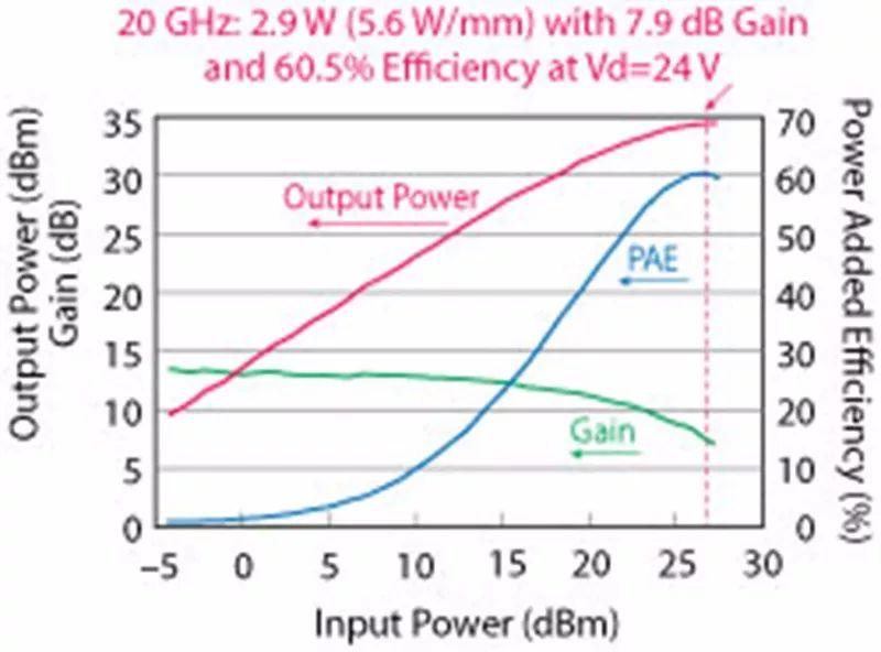
Figure 2: An example device using a 2.9 W (5.6 W/mm) HEMT with a gain of 7.9 dB has a PAE of 61% and a bias point of 24 V
Figure 3 shows the temperature distribution from the center to the edge of the 10-finger HEMT of different types of GaN-on-diamond wafers. Akash Systems uses "gradient diamond with low thermal boundary resistance (TBR)" to make GaN on diamond (green); this curve shows a peak temperature of 152°C (the first peak). The temperature of GaN on SiC at the same point on the device is 232°C.
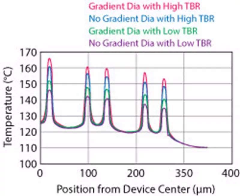
Figure 3: Shows the temperature distribution from the center of the channel to the edge of a 10finger HEMT wafer of GaN on diamond of different types
Akash Systems plans to launch a 24kg 12U (36cm x 24cm x 23cm) satellite system into LEO orbit in 2019. It will include a 20-watt signal transmitter based on a diamond-based GaN power amplifier. The system will exhibit a landmark 14gbps data rate, which is unique for a satellite system of this size.
Future prospects of GaN on diamond
Introducing diamond into high-frequency, high-power GaN-based microwave power devices and circuits to solve the heat dissipation problem of the devices has been an international research hotspot in recent years. Polycrystalline diamond-based substrate transfer technology, single crystal diamond-based material direct epitaxy technology, and nano-diamond film-based device surface coating technology have very important applications in solving the heat dissipation of high-frequency and high-power GaN-based HEMTs potential.
The next generation of diamond-based GaN technology will support future high-power radio frequency and microwave communications, aerospace and military systems, paving the way for 5G and 6G mobile communication networks and more complex radar systems.
GALOCE various kinds range of strain gage static torquemeters, allowing to measure in the two directions from ± 0.1 Nm up to ± 5000 Nm with high accuracies (1%). Using standard din flanges. This torque sensors are usually used for measuring tightening torques, verify and calibrate screw driving systems and dynamometric torque wrenches. Click here, if you are interested in Dynamic Torque Sensor.
Static Torque Sensor,Static Torque Transducer,Torque Measurement Sensor,rotary torque sensor
GALOCE (XI'AN) M&C TECHNOLOGY CO., LTD. , https://www.galoce-meas.com