Simulation and eye diagram embedding and de-embedding test methods in high-speed circuit design
Signal integrity is a system engineering that analyzes and mitigates the negative effects of noise, distortion, and loss in high-speed digital links, and is an important guarantee for high-speed link performance and system-level reliability. However, how to ensure the integrity of electrical performance is a major problem in the high-speed circuit "Siege Lion". Skilled "old birds" can always apply signal integrity theory and use simulation and test tools reasonably to quickly solve various circuit problems.
Today, let's talk to you about the tools and provide hands-on videos to make everyone's technology "suddenly advance."
In high-speed digital signal transmission, a channel refers to an electronic path from a transmitting end IO Buffer to a receiving end IO Buffer. It may consist of a chip package, traces on the PCB, connectors and cables. A simple channel can be routed from the transmitter IO Buffer, PCB to the receiver IO Buffer. A complex channel (such as a backplane) consists of the components shown in Figure 1.
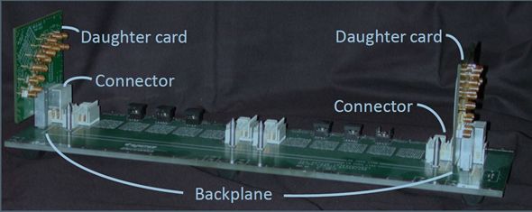
â–² Figure 1. A channel about 20 inches long
When modeling the channel
Need to pay attention to the three most important features
1. Impedance; 2. Loss; 3. Delay or phase
The impedance depends on the mechanical structure, dielectric constant and metal conductivity. Impedance mismatches cause multiple reflections that eventually cause signal ringing, overshoot, and undershoot.
In addition, channel loss is critical to SERDES design. The main causes of signal loss are dielectric loss and conductor loss, which are usually frequency dependent. Thus the bandwidth of a channel limits the maximum bit rate it can pass. For DDR, the phase difference between command, address and clock or DQ and DQS must be well controlled.
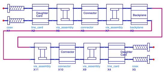
â–² Figure 2. Different components in a channel
The components of the channel can be modeled using a formula-based transmission line model, an electromagnetic model, or a measurement-based model. The correctness of modeling for each component depends on the size and accuracy of the material parameters. Once the component model is accurately defined, these components are cascaded to create a complete channel model (shown in Figure 2), and the impedance and delay of the channel can be estimated by TDR simulation (as shown in Figure 3). The insertion loss of the channel can be estimated by S-parameter simulation (as shown in Figure 4). Ultimately, these simulation results will provide debugging optimization clues for the “Siege Lion†to improve channel performance and support higher rate transmission.
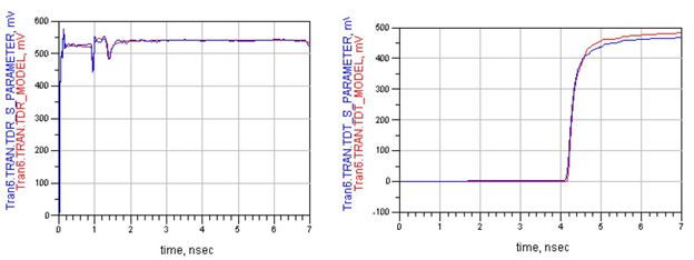
â–² Figure 3. Impedance change (left) and time delay (right)
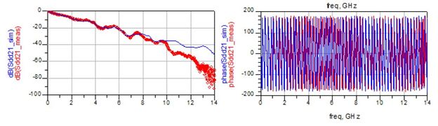
â–² Figure 4. Insertion loss (left) and phase (right)
Seeing that the small partners here basically understand the method of high-speed channel modeling, right? But how do you do it? The video below will teach you "Build a high-speed channel model with a specific frequency loss."
(Want to learn more about ADS for signal integrity and power integrity analysis? Details are available later)
After reading the friends, is there any confidence in using ADS to build a high-speed channel model? By constructing the channel model, I can adjust the link parameters at will, to see the impact of these parameters on the parameter representation of the model, and finally find the optimal solution.
After the simulation optimization of the link is completed, it is inevitable to apply the optimized result to the specific circuit, and perform necessary debugging according to the actual situation of the circuit to ensure that the actual result of the product is in line with expectations. At this stage, Keyisght's oscilloscope is a very necessary test tool, which can easily and accurately test and characterize various indicators of circuit signals, speeding up test verification.
Of course, "old birds" are often not satisfied with this, but also think about how to "predict" the effect before the new board proofing, improve the optimization efficiency, reduce the number of investment, and shorten the product launch cycle. The Keysight oscilloscope can provide another debugging "artifact" - the oscilloscope offline software N8900A.
After using ADS for link simulation and obtaining S parameters, the model can be imported into the N8900A, and the measured signal eye diagram of the high-speed link front end is embedded and de-embedded to facilitate the evaluation of the high-speed link model of the Siege Lion. The impact of real signals, thus finding clues and directions for debugging.
2D Scanner ,2D Wired Barcode Scanner,2D Barcode Scanner Online,2D Code Scanner
ShengXiaoBang(GZ) Material Union Technology Co.Ltd , https://www.sxbgz.com