The Basic Principle of Hall Effect Discusses the Calibration Problem of Hall Probe Replacement
The meter can complete the measurement of stable field, pulse field peak, alternating field positive and negative peak, peak-to-peak and its frequency. It also has automatic measurement function.
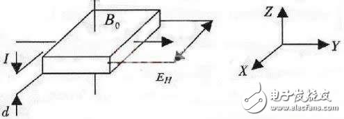
Figure 1: Hall Effect Schematic
Measuring principle
The basic principle of the Hall effect is shown in Figure 1. A current I is applied in the Y direction, and a magnetic field having a magnetic induction intensity of 90 is applied in the Z direction. Then, the carriers are subjected to a Lorentz force in the X direction to generate a Hall electromotive force EH at both ends. A Hall device manufactured according to a Hall effect is a semiconductor wafer having a certain shape, and its Hall electromotive force is:
EH=RH(IB0/d)(1)
In the formula, RH is the material-related Hall coefficient, d is the thickness of the Hall device, I is the current flowing through the Hall device, and Bo is the magnetic induction intensity of the external magnetic field. For a Hall device, in the case where the current I is constant, EH is proportional to the external magnetic field Bo, and a proportional coefficient K=RH is set. Therefore, for different Hall sensors, the operating current I can be changed to have the same scaling factor.
The calibration of the Hall device is to determine the proportional relationship between the Hall electromotive force EH and the external magnetic field Bo. Therefore, in the linear region of the Hall device, by changing the operating current I, it can reach the preset proportional relationship between the Hall electromotive force EH and the external magnetic field Bo, thereby completing the calibration of the linear region. The data table of the non-linear area Hall electromotive force and the external magnetic field Bo under the corresponding operating current is stored in a serial E2PROM, and the external magnetic field Bo can be obtained through a lookup table and a linear fitting method during the measurement. Therefore, simply package a serial E2PROM on the Hall device probe and store the probe's operating current and the corresponding non-linear area table. After replacing the probe, the CPU of the magnetic field measuring instrument can obtain the operating current of the probe from the E2OPROM, and then adjust a controlled constant current source to complete the calibration work.
hardware design
The hardware circuit of the instrument is mainly composed of a main control circuit, a calibration circuit, a signal processing and acquisition circuit, and a frequency measurement circuit.
Master control circuit
The main control circuit takes AT89C52 as the core, including a dual channel A/D converter MAXlll, two D/A converters MAX541, 8279 extended keyboard display circuit, a calibration parameter memory X24128 and RS232 interface to communicate with the host computer. . In order to reduce the interference, an opto-isolation circuit is added between the analog circuit and the digital circuit.
One of the A/D converters MAXlll is used to detect the output of the zeroing circuit, and the other is used to acquire the sensed voltage signal after it is held. One of the two D/A converters, the MAX541, is used to output the offset voltage of the Hall nonequal potential, and the other is used to control the voltage controlled constant current source.
The 8279 extended six buttons: power button, calibration button, zero key, range conversion key, automatic measurement key, display pause key, the keyboard to work in an interrupt mode. At the same time, through the 8279 expansion of the dual 8-bit digital head, one used to display alternating magnetic field frequency, and the other by software control to display different values ​​according to different magnetic fields. When the steady field is measured, the magnetic field value is displayed; when the pulse field is measured, the peak value is displayed; when the alternating magnetic field is measured, the positive and negative peaks and peak-to-peak values ​​are displayed in sequence by the software, and the display time interval is controlled by the software to be 5s. Hold down the display hold key, keep the current display data, press the display hold key again to display the next data.
The parameter memory X24128 is packaged with the Hall device and connected to the host through a serial bus.
Calibration circuit design and working principle
The calibration circuit consists of a voltage-controlled constant current source and a D/A conversion circuit that provides a control voltage. The voltage-controlled constant current source is composed of two high-resistance dual operational amplifiers LM358. The schematic diagram is shown in Figure 2.
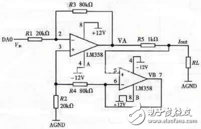
Figure 2: Schematic diagram of voltage controlled constant current source
From the figure can be drawn:
Iout=—4VIN(mA)
In the formula, VIN is provided by 16-bit D/A converter MAX541, can adjust in 0- 2.5V with 0.04mV resolution. Therefore, the constant current source current can be adjusted with a resolution of 0.161 μA between 0 and 10 mA, which can fully satisfy the constant-current operation requirements of the general Hall device.
Signal Processing and Acquisition Circuits
In order to carry out high-precision measurement of different types of magnetic fields, the signal processing circuit of this system consists of a program-controlled amplification circuit, a digital zero-adjustment circuit, and a peak detection and hold circuit. The processed signal is collected by MAX1ll channel 1.
Digital zeroing circuit
Due to the manufacturing process, Hall devices always have unequal potentials. In order to meet the needs of automatic measurement, the compensation of inequality voltage is realized by the digital zeroing circuit. The schematic diagram is shown in Figure 4. This circuit is actually an addition and subtraction circuit composed of two operational amplifiers. When the system is initialized, zero is adjusted for different ranges, and the corresponding compensation voltage value is stored in RAM. After the range conversion or manual range selection in the measurement process, the corresponding value can be directly queried and the D/A converter outputs the compensation voltage. . Due to the use of high-precision A/D and D/A converters, the unequal potential after zeroing is less than 0.1mV.
Peak detection and hold circuit
In order to measure the peak value of the pulsed magnetic field and the alternating magnetic field, the system includes a positive and negative peak detection and hold circuit composed of a sample and hold device LF398 [5] and a logic control circuit. Positive peak detection and hold circuit schematic shown in Figure 5. LF398 control terminal 8 logic value E = (A + B) * D, when E is high, LF398 is in following state, the output voltage is equal to the input voltage; when E is low, LF398 is in the hold state, the output remains unchanged. The operation of the peak hold circuit is: when data acquisition is performed, P2.0 is set to low level and P2.1 is set high, so that the control side of the LF398 depends entirely on the output of the LM319 comparator. The output level of the LM319 can be determined by comparing the output voltage Vo of the LF398 with the input voltage Vin. When the input voltage Vin is higher than the output voltage Vo, the logic control of the LF398 is set to a high level so that the LF398 is in a follow state; when the input voltage Vin is lowered to a peak, the logic control terminal of the LF398 is set to a low level. Keeping the LF398 in hold maintains the "peak" hold. In the sample state, in order to keep the peak value not to be washed off by the next different peak, when P1.2 is detected to be set to low level (the LF398 has achieved the peak value), the P2.1 pin is set to the low level. This blocked the input signal. When measuring a constant magnetic field and an alternating magnetic field, it is often necessary to change the range in order to increase the accuracy. After each range conversion, P2.0 and P2.1 are first set high to make the LF398 in the follow state with a delay of 50 μs, which makes the output and input of the LF398 equal; then P2.0 is set low to enter the peak detection state. Complete range conversion.
The negative peak detection circuit only adds an inverter before the positive peak detection circuit, and the logic control part is completed by P1.3, P2.2, P2.3. The peak held down is detected by channel 1 of MAX1ll after an analog switch CD4051.
Frequency measurement
Since the AT89C52 contains three timing counters, the measurement frequency is very simple and convenient. It only needs to properly amplify the output signal after the zero adjustment, and then after a zero-crossing comparator, the square wave signal is obtained after being shaped, and then passes a frequency division of four. The input to the AT89C52 counter T1 and the external interrupt INT0 can be. In order to measure the frequency more accurately, when the signal frequency is higher than 5kHz, use the frequency measurement method, that is, interrupt INT0, set the timer TO to a time to, open the counter T1, and the counter overflows once, then add a unit in the memory. 1; If the count value in the to time is N1, the frequency of the measured signal can be obtained as 4Nl/to. When the frequency is lower than 5kHz, the cycle method is used, that is, the counter T1 is turned off, the timer TO is started, and the interrupt INT0 is triggered in an edge manner. When the first interrupt occurs, the TO time is t1. When the interrupt occurs again, the interrupt is turned off. At this time, the counter is interrupted. When the TO time is t2, the period of the signal to be measured is T=(t2-t1)/4 and f=4/(t2-t1). To measure a lower signal frequency, TO cycles can be counted. Due to the addition of a divide-by-four, the method can measure signals less than 2MHz.
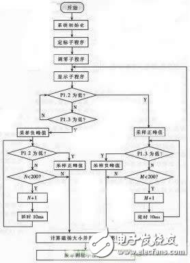
Figure 3: Instrument Software Flow Chart
Instrument software design
The instrument software is written in assembly language, including main program, calibration subroutine, zero adjustment subroutine, data acquisition subroutine, display subroutine, keyboard interrupt service routine, frequency measurement program, A/D conversion program, D/A conversion. Procedures, calculation of magnetic field size subroutines, etc. The system defaults to automatic measurement mode, select the maximum range. In the keyboard interrupt program, different keys are pressed to execute different programs. In the data acquisition subroutine, determine whether it is manual, if it is, then directly collect and save the data. If not, judge whether the measuring range is appropriate. If it is not appropriate, re-measure the conversion range and save the previous measurement value. If the measurement is zero after conversion, it means the pulsed field. The value of the above measurement is correct. Therefore, for pulse fields, if you know the field strength range, it is best to manually select the range. Instrument software flow chart shown in Figure 3.
The single-chip microcomputer is used as the core of the measuring instrument. The serial magnetic memory is used to expand the measuring range of the magnetic field, and the pressure-controlled constant current source technology is used to solve the calibration problem after the replacement of the Hall probe. The instrument has an automatic range conversion function, and can simultaneously measure the magnetic field frequency, its magnetic field measurement range: 0.01mT ~ 6T, measurement accuracy is better than ± 0.2% of the measuring range, especially for large magnetic field, unknown type of measurement occasions.
30 Inch Aio,Aio Computer,30 Inch All In One Pc,All In One Pc Adapter
Guangzhou Bolei Electronic Technology Co., Ltd. , https://www.nzpal.com