Building Distributed RAM Using LUT in 3 Series FPGAs (2)
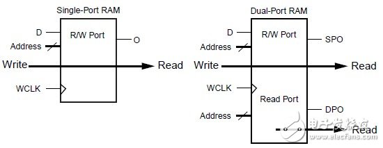
Distributed RAM supports the following single-port RAM and dual-port RAM types:
SRAM with asynchronous write/synchronous read, where synchronous reads can be implemented using flip-flops associated with distributed RAM.
A DRAM with one synchronous write port and two asynchronous read ports, wherein the principle of synchronous synchronous read is the same as the former.
Figure 1 shows an illustration of SRAM and DRAM. It can be seen that the DRAM has a read/write port and a separate read port. Any write operation to the D input port and read operation to the SPO output port can be performed simultaneously and independently of the read operation of the other read port, the DPO.
If the read and write operations occur at the same time, the data reflected in the memory unit is output when the data is written synchronously. This mechanism is similar to the mechanism of the block RAM in the Spartan-3 series FPGA. The User Guide is called "WRITE_MODE=WRITE_FIRST". Figure 2 shows the timing diagram for this operation.
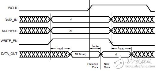
Only one clock edge is required for a write operation.
Read operations only require a logical read time.
The output is asynchronous and its delay is only related to the logical delay of the LUT.
Data and address inputs are stored on the write clock and have specific settling time requirements, but do not require hold time.
The A[#:0] ports of the dual port RAM are read and write addresses, and the DPRA[#:0] ports are independent read-only addresses.
Smart Terminal,Cba Smart Terminal,Smart Payment Terminal,Pos Smart Terminal
Guangzhou Winson Information Technology Co., Ltd. , https://www.barcodescanner-2d.com