FPGA Learning: Power Circuit Design
As with any electronic component, FPGA devices require a supply voltage supply to operate. Especially for larger devices, their power consumption is relatively high, and the power supply system will directly affect the stability of the entire development system. Therefore, designing an efficient, high-performance FPGA power supply system is of great importance.
Different FPGA devices and different application modes have different voltage and current requirements. As shown in Figure 2.4, a simple summary can be divided into three categories of voltage requirements for FPGA devices: core voltage, I/O voltage, and auxiliary voltage.

Figure 2.4 Supply Voltage for FPGA Devices
The core voltage is the basic voltage required for normal operation of various logic circuits in the FPGA. This voltage is used to ensure the FPGA device itself. Usually selected a certain FPGA device, the core voltage is generally a fixed value, will not change because of different applications of the circuit. The core voltage value can be found in the official device manual.
The I/O voltage is, as the name implies, the reference voltage needed by the FPGA's I/O pin to operate. In the pin arrangement, the FPGA is different from the ASIC in that the available signal pins of the FPGA can all be used as ordinary I/O. The level of the level is completely determined by the internal logic of the device. Of course, its high and low levels are also limited by the supplied I/O voltage. For any FPGA device, its I/O pins are usually divided into multiple banks according to the arrangement position. The I/O voltages supplied by all the I/O pins in the same bank are common and can provide different I/O voltages to different banks. They are disconnected from each other. Therefore, different I/O voltages of different banks provide flexibility for different interface applications of FPGA devices. As an example, some banks in the Cyclone IV family of devices support the LVDS differential level standard. The device manual will require the designer to supply 2.5V to the I/O voltage of the banks used for LVDS differential applications. General LVTTL or LVCOMS 3.3V power supply requirements. Once these I/O banks for LVDS transmission are supplied with 2.5V, they cannot be used as 3.3V or other standard transmissions.
In addition to the aforementioned core voltages and I/O voltages, other voltages required for the operation of FPGA devices are often referred to as auxiliary voltages. For example, the FPGA device downloads and configures the required voltage. Of course, the auxiliary voltage value here may be the same as the core voltage value or the I/O voltage value. Many FPGAs have special requirements for the power supply of the PLL block, which can also be considered as an auxiliary voltage. Since the PLL itself is an analog circuit, and the circuit in other parts of the FPGA is basically a digital circuit, the input power supply voltage of the PLL is also very particular, and a special capacitor circuit is required to perform filtering processing, and its voltage value and I/O voltage value are general. different. In addition, Cyclone V GX series FPGA devices with high-speed Gbit serial transceivers, for example, usually have an additional reference voltage; the MAX10 series device ADC function pin circuits also require an additional reference voltage; some FPGA pins with DDR3 controller function There are usually dedicated reference voltages on the same... Reference voltages such as this one can be classified as the auxiliary supply voltage of the FPGA and must be considered during the actual power supply circuit connection and design process.
The current common power supply solutions are mainly LDO regulators, DC/DC chips or power supply modules. The LDO regulator has the characteristics of simple circuit design and low output power supply voltage ripple, but its obvious disadvantage is its low efficiency. The DC/DC chip-based solution can ensure high power conversion efficiency and heat dissipation. It is easier and the output current is larger. It is the best choice for large-scale FPGA devices. The power supply module is simple and practical and can have more stable performance, but the price is usually more expensive. In the case of insensitive cost requirements, it is FPGA. One of the simplest and fastest solutions for power supply design. Judging from the author's many years of experience, the following principles are generally followed in the selection of LDO regulators, DC/DC chips, or power supply modules:
â— Voltages lower than 100mA can be considered for use with LDO regulators because of the simplicity of the circuit, the use of fewer components, the small footprint of the PCB, and the relatively low cost.
â— Consider the use of LDOs for power supply ripple-sensitive power supplies such as analog supply voltages for CMOS sensors and reference voltages for ADC chips.
â— In addition to the above situations, the general current is large and the requirement for the power supply voltage ripple is not high. DC/DC circuits are considered as far as possible. After all, it can provide high-current power supply and provide the best power conversion efficiency.
â— For the power supply module, I see the most is the use of military and other cost-insensitive, board-level PCB space applications, it is in fact the integration of LDO regulator and DC / DC circuit advantages.
Generally speaking, for the selection of the power supply scheme of the FPGA device and the design of the power supply circuit, it is necessary to make preliminary preparations in advance. The following points must be considered:
â— The device needs to supply several voltages. What is the pressure value?
â— What is the maximum current requirement for different voltage ranges?
â— Is there a power sequence requirement for different voltage ranges? (Most FPGA devices do not have this requirement)
â— How to allocate and arrange the power supply decoupling capacitors?
â— Does the power supply voltage require a special decoupling circuit?
The various electrical parameters and power supply design considerations that the designer needs to determine are generally referenced in the device handbook, applica T I notes, or white paper provided by the device manufacturer. design. Therefore, if the designer wants to be able to better complete the power supply circuit design of the FPGA device, it is necessary to read a large number of official documents in advance.
When it comes to power supplies, we can't help but mention the design of the ground (GND) circuit. The ground signal of the FPGA device is usually paired with the voltage. In general applications, there is no problem in the unified common ground connection, but it also needs to pay attention to whether there are isolation requirements in special applications. The ground signal from the pin of the FPGA device is usually turned on. Of course, exceptions cannot be ruled out. If the signal is dropped, the device usually works normally, but I also encountered some special conditions. For example, there is a grounding pad in the center of the bottom of Altera's Cyclone III device. If the ground signal is ignored in the design, then The FPGA is likely not to work because the ground signal is the ground of many intermediate signals that are connected to the FPGA. It is not directly connected to other ground signals of the FPGA. Therefore, in the design, we must also pay attention to the connection of the ground signal. Any slight oversight of the power supply circuit may cause the device to strike.
On this experimental platform we designed, as shown in Figure 2.5, powered by the USB port of the PC, it can usually provide 5V/0.5A voltage and current. The 5V voltage input to the two DC/DC circuits generates 3.3V and 1.2V, respectively, and the DC/DC chip can support a maximum current of 3A. Of course, our FPGA device does not actually require such a large current. The reason why the DC/DC circuit is used to generate 3.3V and 1.2V voltage is considering that 3.3V is the I/O voltage of the FPGA, and it is also the supply voltage of most of the peripherals on the board. Its current is relatively large; and 1.2V is FPGA devices have higher voltages and currents; therefore, they use DC/DC circuits that are more suitable for both larger current demands and better power conversion efficiency. The 2.5V to 2.5V LDO circuit is used because the 2.5V is only used by the FPGA configuration circuit, the current is relatively small, it does not require high conversion efficiency, use a simple LDO circuit to be more "economical Affordable "some.
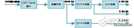
Figure 2.5 Power Circuit Diagram
As shown in Figure 2.6, this is a layout diagram of the power circuit. In order to obtain greater current supply capability and higher power conversion efficiency, we can only use more discrete components and larger layout space to " compromise".
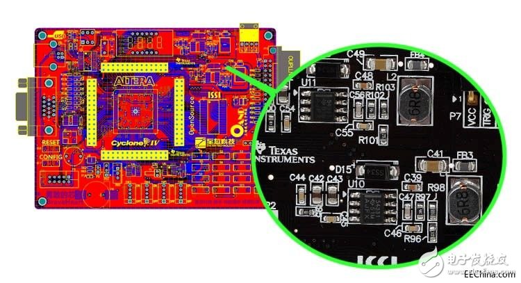
Figure 2.6 layout of the power circuit
5*20MM 6*30MM fuse holder fuse holder fuse holder
Suitable for 5.0 * 20MM fuse
Applicable current: 10A / 250V t-25 to t-70Material: insulator E130i UL 94-V0
Environmental protection products, certified by CE UL VDE CQC
Fuse (fuse), self recovery fuse (PPTC), ESD suppressor, etc.
It is widely used in a variety of electronic and electrical equipment, such as: computer and its peripheral equipment, LCD, battery pack, communication system, audio equipment, automotive industry, testing instruments, industrial control power supply and frequency converter, etc.
Fuse Holder
ShenZhen Antenk Electronics Co,Ltd , https://www.antenk.com