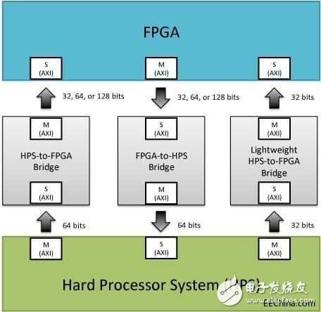
The structure of interconnection between FPGA and HPS
This week I want to further explore the structure of the interconnection between programmable logic (FPGA) and hard processor (HPS). I discovered three main ways how they map and handle communications, which components need to manage timing and have access.
AXI BridgeIn order to realize the communication interface between HPS and FPGA, the AXI bridge protocol was derived. The AXI bridge protocol handles bandwidth adaptation and clock control and supports bi-directional logic and data interaction between the HPS and the FPGA.

There are two types of HPS to FPGA: high throughput and low throughput. The high-throughput data bandwidth can be 32-bit, 64-bit, or 128-bit, which is designed specifically for high-bandwidth data transmission. HPS is the master and is at the L3 layer.
The lightweight (or low throughput) channel is limited to 32 bits, however it is optimized with minimal delay. Its main function is to pass control and status registers to the FPGA. In addition, it also performs a certain flow splitting of the HPS-to-FPGA communication channel. The specific analogy description is shown in Figure 1. There are two channels from the HPS to the FPGA: the first is that the 32-bit data channel has a higher speed limit, and the other is A large number of channels are designed to support higher bandwidth and more data transmission at the same time.
FPGA to HPSThe third channel in Figure 1 is to implement FPGA-to-HPS data transfer. It is designed to access the HP slave interface or wait for data input on the HPS program. It can be configured as a 32-bit, 64-bit, or 128-bit data bandwidth that is controlled by the HPS L3 main switching clock.
In order to combine these communication channels, I began to look through the Intel Hardware Developer's Guide to the Golden Hardware Reference Design (GHRD), which provides examples of how to establish an AXI bridge channel between FPGAs and HPS. Really realized the powerful function of "Configuration Wizard", I only need six mouse clicks to complete the configuration of the three communication channels, and you can also configure the memory allocation. Finally I learned that the HPS bridge is mapped to on-chip memory to achieve as little latency as possible. The FPGA part is mapped to a slave memory address and writes data to memory when there is data.
Integrate them togetherWhat does this mean? Communication channels and different transport layers do not have too many opportunities for me to use them for those who are experienced in small low-power MCUs. However, developers who are accustomed to ARM MCU programming may be familiar with these communication bridges. In fact, these communication channels are a series of control registers and memory maps that are accessed at very high speeds. This is very useful for multi-threaded, multi-core systems because such systems require high-speed, multi-purpose data transfer. Of course, this kind of interconnected idea is very common for MCU enthusiasts. Using internal interconnect communication channels to share tasks is very familiar, but accessing them as memory or RAM is somewhat novel. In simple terms, the L3 layer is designed to implement the communication mechanism from the FPGA to the HPS and supports data transfer between different processor cores. It opens up the FPGA resources to perform some of the tasks that the HPS has to accomplish, otherwise the HPS will be greatly hindered, ultimately improving the overall system performance.
Power 30W ,output voltage 3-12V, output current Max 1.2A , USB output 5v 2a, 6 dc tips. We can meet your specific requirement of the products, like label design. The material of this product is PC+ABS. All condition of our product is 100% brand new.
Our products built with input/output overvoltage protection, input/output overcurrent protection, over temperature protection, over power protection and short circuit protection. You can send more details of this product, so that we can offer best service to you!
30W Wall Adapter ,30W Wall Power Supply,30W Power Cord In Wall, 30W Wall Power Adapter
Shenzhen Waweis Technology Co., Ltd. , https://www.waweisasdapter.com