Third-generation semiconductor material characteristics and information
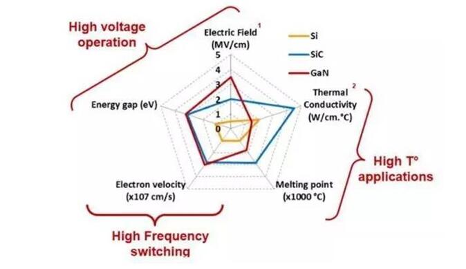
Compared with the first and second generation semiconductor materials, the third generation semiconductor material has a wider band gap, higher breakdown electric field, higher thermal conductivity, higher electron saturation rate, and higher radiation resistance (Figure 2) is more suitable for making high-temperature, high-frequency, anti-radiation and high-power devices. It is usually called wide-bandgap semiconductor material (with a band gap of more than 2.2 eV) and is also called a high-temperature semiconductor material. From the current third-generation semiconductor materials and devices research, the more mature is SiC and GaN semiconductor materials, and zinc oxide, diamond, aluminum nitride and other materials research is still in its infancy. Silicon Carbide (SiC) and Gallium Nitride (GaN)—also known as the duo of third-generation semiconductor materials.

Figure 2 Material characteristics of third-generation semiconductors
Compared with Si, SiC has many advantages: it has 10 times electric field strength, 3 times higher thermal conductivity, 3 times wider forbidden band width and 1 times higher saturation drift speed. Because of these characteristics, devices made of SiC can be used under extreme environmental conditions. Microwaves and high-frequency and short-wavelength devices are currently mature application markets. The 42GHz frequency SiCMESFET is used in military phased-array radars and communication broadcasting systems. High-brightness blue LEDs using SiC as a substrate are key devices for full-color, large-area displays.
Doping nitrogen or phosphorus in silicon carbide SiC can form n-type semiconductors, while doping aluminum, boron, tantalum, or niobium forms p-type semiconductors. The heavy doping of boron, aluminum, or nitrogen in silicon carbide can provide doped silicon carbide with an electrical conductivity comparable to that of metal. The Al-doped 3C-SiC, B-doped 3C-SiC, and 6H-SiC SiC all have superconductivity at a temperature of 1.5K, but the magnetic field behavior of both Al and B-doped SiC The obvious difference. Aluminum-doped silicon carbide is a type II semiconductor like B-doped crystalline silicon, but boron-doped silicon carbide is an I-type semiconductor.
Gallium Nitride (GaN, Gallium Nitride) is a compound of nitrogen and niobium. The structure of this compound is similar to wurtzite and its hardness is high. As a new emerging semiconductor process technology, it offers many advantages over silicon. Compared to silicon devices, GaN achieves a performance leap in power conversion efficiency and power density.
GaN has excellent breakdown capability, higher electron density and speed, and higher operating temperature. The GaN has a wide energy gap of 3.4 eV and is widely used in power factor correction (PFC), soft-switching DCDC and other power supply system designs, as well as power adapters, photovoltaic inverters or solar inverters, servers, and communications power supplies. Terminal area.
GaN is an extremely stable compound. It is also a hard, high-melting material. It has a melting point of about 1700°C. GaN has a high degree of ionization and is the highest among the Group III-V compounds (0.5 or 0.43). Under atmospheric pressure, the GaN crystal is generally a hexagonal wurtzite structure. It has 4 atoms in a cell, and its atomic volume is about half that of GaAs. Because of its high hardness, it is also a good coating material.
The electrical properties of GaN are the main factors affecting the device. Unintentionally doped GaN is n-type in all cases, and the best sample has an electron concentration of about 4 x 10¹⁶/cm3. In general, the p-type samples prepared are highly compensated.

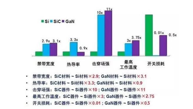
Figure 3 shows the characteristics of Si, SiC and GaN semiconductors
Third generation semiconductor material properties and applicationsThe development of the semiconductor industry has gone through three stages. The first generation of semiconductor materials is represented by silicon (Si). Second-generation semiconductor materials, gallium arsenide (GaAs), have also been widely used. The third-generation semiconductor materials represented by gallium nitride (GaN), silicon carbide (SiC), and zinc oxide (ZnO), etc., have significant performance advantages and are widely acclaimed in the industry, compared with the previous two generations. The third-generation semiconductors are characterized by high breakdown electric field, high saturation electron velocity, high thermal conductivity, high electron density, and high mobility. Therefore, they are also known in the industry as “core cores†for solid-state light sources, power electronics, and microwave radio frequency devices. The "new engine" of optoelectronics and microelectronics industries. The well-developed wide bandgap semiconductors are mainly SiC and GaN, in which the development of SiC is earlier. Some parameters of SiC, GaN, Si, and GaAs are shown in the figure below:
It can be seen that the forbidden band widths of SiC and GaN are much larger than Si and GaAs, and the corresponding intrinsic carrier concentration is lower than that of Si and GaAs. The maximum working temperature of wide bandgap semiconductors is higher than that of the first and second generation semiconductor materials. Breakdown field strength and saturation thermal conductivity are also much larger than Si and GaAs. Taking SiC as an example, it has a wide band gap, high breakdown electric field, high thermal conductivity, high electron saturation rate, and higher radiation resistance, and is very suitable for making high temperature, high frequency, and radiation resistance. High-power devices.
Products are accepted by the market, and price and performance are the main considerations. The performance of SiC is undoubted, but its cost is still higher than that of silicon products. Under the same characteristics, the same voltage, and the same conditions of use, it will be about 5-6 times more expensive than silicon products. Therefore, at this stage only high performance is required. And applications that are not very price-sensitive are beginning to replace silicon products such as automobiles, car charging posts, and solar energy. To replace silicon products, SiC still has a lot of room for development. When the cost of SiC can be reduced to 2 to 3 times that of silicon, it should result in a large market size. By 2020, when EVs are launched on a large scale, the SiC market will have an explosive growth.
In terms of applications, according to the development of third-generation semiconductors, its main applications are semiconductor lighting, power electronics, lasers, and detectors, as well as other four fields. The maturity of each industry varies, as shown in the figure below. In the frontier research field, wide bandgap semiconductors are still in the laboratory development stage.

Reviewing the development of the semiconductor industry, it successively experienced the first generation of semiconductor materials represented by silicon (Si) and the second generation of semiconductor materials represented by gallium arsenide (GaAs). In the last century, the two generations of semiconductors Materials have made great contributions to industrial progress and social development. Today, wide bandgap semiconductor materials typified by gallium nitride (GaN), silicon carbide (SiC), zinc oxide, diamond, and aluminum nitride are collectively referred to as third generation semiconductor materials.
As a new type of wide bandgap semiconductor material, the third generation of semiconductor materials has advantages unmatched by the previous two generations of semiconductor materials in many fields of application: such as high breakdown electric field, high saturation electron velocity, high thermal conductivity, high electron density, Features such as high mobility can realize high-voltage, high-temperature, high-frequency, and high-radiation-resistance capabilities. It is known as the "core" of solid-state light sources, power electronics, and microwave radio-frequency devices. It is a "new engine" for optoelectronics and microelectronics industries. .
From the scope of application, the third-generation semiconductor field also has the characteristics of strong interdisciplinarity, wide application fields, and large industrial connections. It has broad application prospects in semiconductor lighting, next-generation mobile communications, smart grids, high-speed rail transit, new energy vehicles, and consumer electronics, and is a key new material supporting the development of industries such as information, energy, transportation, and national defense.
As a key device for the new generation of semiconductor lighting, the third generation of semiconductor materials also has a wide range of basic and important leads. Judging from the current research on third-generation semiconductor materials and devices, the most mature materials are gallium nitride (GaN) and silicon carbide (SiC) semiconductor materials, and they are also the two most promising materials.
Compared with the silicon of the first generation semiconductor material, silicon carbide has many advantages: it has 10 times higher electric field strength, 3 times higher thermal conductivity, 3 times wider forbidden band width, and 1 times higher saturation drift speed. Because of these characteristics, it makes it as small as LED lighting, household appliances, new energy vehicles, as well as rail transportation, smart grids, and military-industrial aerospace, all of which have advantages, so the silicon carbide market is quite promising by various industrial circles.
The advantages of direct gallium nitride transitions, high electron mobility and saturated electron velocity, and lower cost make it faster to develop. The different advantages of the two determine the difference in the application range. In the field of optoelectronics, gallium nitride occupies an absolute dominant position, while in other power devices, silicon carbide is suitable for high-temperature and high-power fields of over 1200V, and GaN is more suitable for 900V. The following high-frequency small power areas. Can have their own advantages.

Under the stimulation of great advantages and bright prospects, all countries in the world are now increasing the horsepower distribution of the third generation of semiconductors, but China's progress in wide-bandwidth semiconductor industrialization is still relatively slow, and wide bandgap semiconductor technology urgently needs to be broken.
“The biggest bottleneck is raw materials.†Wang Xiaoliang, a researcher at the Institute of Semiconductor Research at the Chinese Academy of Sciences and the secretary general of the Semiconductor and Integrated Technology Subcommittee of the Chinese Institute of Electronics believes that the quality and preparation of raw materials in China needs to be solved. In addition, Zeng Jianping, associate professor of applied physics at Hunan University, also stated that at present, the preparation of SiC wafers in China is still vacant, and most of the equipment is imported.
"The domestic research on SiC and GaN materials and devices is relatively late. Compared with foreign countries, the level is relatively low, and an important factor that hinders the progress of domestic third-generation semiconductor research is the original innovation." National Semiconductor Lighting Engineering R&D and Industry Alliance I Experts said that most of the domestic research institutes and related manufacturing companies in the field of new materials are eager for quick success and are unable to tolerate the long-term “only input, no output†status. Therefore, the original innovation of new materials represented by the third generation of semiconductor materials is difficult.
Original innovation is an innovation process from scratch, characterized by large investment and long cycle. Taking SiC as an example, it has a wide forbidden band width, high breakdown electric field, high thermal conductivity, high electron saturation rate, and higher radiation resistance, and is very suitable for making high temperature, high frequency, and radiation resistance. High-power devices. However, it is very difficult to grow SiC crystals. After decades of research and development, only a few companies such as American Cree Corporation, German SiCrystal Corporation, and Japan’s Nippon Steel Corporation have mastered the growth technology of SiC. , Can produce better products, but there is still a long way to go from the actual application of large-scale industrialization. Therefore, the original innovation of new materials, represented by the third generation of semiconductor materials, is difficult to achieve and is a major achievement in industrialization.
“The third generation of semiconductors will have a very big impact on the future industry of our country. The research of its application technology is more crucial. If the related supporting technologies and products cannot keep up, the role and efficiency of third generation semiconductor materials and devices may play a role. It is not good, so it is necessary to develop the whole industry chain in a coordinated manner, said Zhai Wende, vice president of ZTE.
It is both an opportunity and a challenge. In the future, China's third-generation semiconductor industry will face many problems. As Professor Shen Bo of the Broad Band Gap Semiconductor R&D Center of Peking University put it, the opportunity for the development of third-generation semiconductors in China is very good at the moment, because in the past ten years, driven by semiconductor lighting, GaN has become mature regardless of materials and devices. The degree has been greatly improved, but the third generation of semiconductors still has a long way to go in terms of power electronic devices and radio frequency devices. With the market and industry just starting, we are still faced with huge challenges and we must work together.
Custom Piezoelectric Components
The piezoelectric ceramic sound-generating element, especially a lead-free piezoelectric ceramic sound-generating element, is mainly composed of metal flakes and piezoelectric ceramic flakes. The sound pressure generated by this new structure piezoelectric sounder is proportional to the number of piezoelectric ceramic sheets. By increasing the number of piezoelectric ceramic sheets, the required large sound pressure is easily achieved.
Custom Piezoelectric Components,PZT Elements Soldered Wires,Element of Piezoelectric,Piezoelectric Elements Crystal
Zibo Yuhai Electronic Ceramic Co., Ltd. , https://www.yhpiezo.com