Detailed article on memory access and bus
This article mainly introduces the storage area, bus, and IO devices and other major components to understand how the entire computer works. These things are the hardware that can be seen and touched. Usually when we buy a computer, it is the speed of the CPU, the size of the memory, the parameters of the motherboard chip, and so on.
Memory
We used a simple general-purpose computer model to describe how the CPU works. The CPU executes instructions, and the memory provides instructions and data for the CPU. In this simple model, memory is a linear array of bytes. The CPU can access each memory location for a constant amount of time. Although this model is valid, it does not fully reflect the actual working methods of modern computers.
1.1 Memory System Hierarchy
In the previous introduction, we have always equated memory with memory, but in modern computers, the memory system is a hierarchical structure of storage devices with different capacities and different access speeds. The entire memory system includes registers, Cache, internal memory, and external storage. The following figure shows a hierarchy of computer storage systems. The higher the level, the faster, but the higher the price, the lower the level, the slower the speed, and the lower the price.
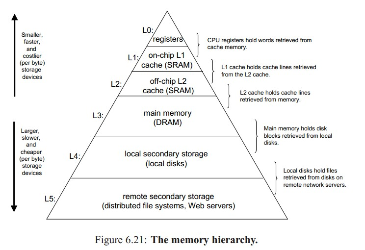
Relative to the CPU, the memory speed is relatively slow. No matter how the CPU develops, the speed is multi-block, and the CPU is always a scarce resource for the computer, so we should use CPU to the maximum degree. On the other hand, we mentioned CPU cycles. One CPU cycle is the shortest time for taking one instruction. This shows that the CPU cycle largely determines the overall performance of the computer. You think about if it takes 2s for the CPU to fetch an instruction, and it takes only 2ms to execute an instruction, it's a huge loss of performance for the computer. Therefore, the speed of the memory has a great influence on the speed of the computer.
For us, we always hope that the speed of the memory can be the same as or as much as possible, so that the clock cycles needed by one CPU cycle will be less. But the reality is that such a computer can be quite expensive. So in the computer's storage system, a hierarchical structure is used. The faster the faster the memory capacity, the better the balance between performance and price.
1.2 Storage Technology
The development of the computer is inseparable from the development of memory. Early computers do not use hard disks and only a few kilobytes of RAM are available. And we now have 4G, 8G memory has been everywhere, 1T's big hard drive and hundreds of G solid-state hard drive, and the price is more than 10 years, 20 years ago a lot cheaper. So I first learned about various storage technologies. Current storage technologies are roughly classified into SRAM memory, DRAM memory, ROM memory, and magnetic disks.
1.2.1 Registers
In the graph of the previous article we have seen that there are many registers inside the CPU, and the previous figure shows that the registers are at the top of the storage hierarchy. It is also called a trigger. It is often clocked with the CPU, so it is very fast. However, a register requires more than 20 transistors, so if used in large quantities, the CPU will be very large. So there are only a few registers in the CPU. Each register is 8-64 bytes in size.
1.2.2 RAM Random Access Storage
There are two types of RAM (Read-Access Memory), static (SRAM) and dynamic (DRAM). SDRAM is much faster than DRAM, but the price is much more expensive.
Static RAM: The SRAM stores each bit in a bistable memory cell, and each memory cell is implemented with a six-transistor circuit. It is characterized by being able to remain in one of the two stable states (just as long as 0 or 1) indefinitely (as long as there is electricity), and any other state that is unstable will immediately switch to these two states. One;
Dynamic RAM: DRAM uses the amount of stored charge in a capacitor to represent whether a binary bit is 1 or 0. Each bit consists of a transistor and a capacitor. In reality, the capacitor will leak, causing the potential difference to be insufficient to cause the memory to disappear. Therefore, unless the capacitor is periodically charged, the memory cannot be guaranteed to last. Because of this need for regular refresh characteristics, it is called "dynamic" memory.
SRAM has lower power consumption than DRAM, but due to its relatively complex structure and large area, it is generally used internally as a cache in CPUs and is not suitable for large-scale integrated use, such as memory. The DRAM is mainly used as the internal memory of the computer.
Cache: At present, we generally integrate two to three levels of Cache in the CPU, and the capacity is from 128K to 4M. For the CPU's total cache, they are also at the same frequency as the CPU, so the theoretical execution speed and registers should be the same, but the Cache is often used to store some instructions and data, so there is a hit problem. When there is no hit, new data needs to be fetched from the next set of memory. At this time, the Cache will be locked, so the actual execution speed is slower than that of the register. Also for L1, L2, L3, the speed is getting slower and slower;
Main memory: That is, we say memory, using DRAM to achieve. However, the memory we currently listen to is generally called DDR SDRAM, and there are early SDRAMs. This is a synchronous DRAM technology, we do not need to understand his details, just need to know that it can effectively improve the DRAM transmission bandwidth. While DDR represents double the rate, and now has DDR2, DDR3, DDR4, their bandwidth is also increasing.
1.2.3 ROM read-only storage
The front RAM will lose data after power off, so they are volatile. On the other hand, non-volatile memory can store data even after a breakpoint. Generally we call it ROM (Read-Only Memory). Although this is said, ROM can still write data under special circumstances, otherwise it cannot be called memory.
PROM: Programmable ROM, which can only be programmed once. The PROM contains a fuse. Each memory cell can only be blown with a high current.
EPROM: Erasable Programmable ROM, with a transparent quartz window. Ultraviolet light is cleared to zero by illuminating the memory cell through the window. Programming it uses a special device to write one. Number of writes 1K times;
EEPROM:: Electronically erasable, programmable ROM that can be programmed directly on a printed circuit board without special equipment. Write 100,000 times;
Flash Memory: This is the flash memory that we see most, including NOR Flash, NAND Flash, V-NAND Flash, SLC, MLC, and TLC. Although based on EEPROM, the speed is much faster. Among them, NOR and NANA Flash are widely used on U disk, SD card and mobile phone storage.
ROM is also used in computers. For example, our BIOS chip uses PROM at first and EPROM later. If it is damaged, it cannot be started. The current mobile phone also uses ROM to burn into the system, and RAM as a memory, using Flash Memory as a body storage.
1.2.4 Disk Storage
This is our most common hard drive. At present, the mainstream of hard disks is already 500G, 1T. The speed is also around 7200 rpm. Compared to 8G memory, a 500G hard drive can be said to be quite cheap. But the problem is that his speed is very slow, reading data from the disk takes a few milliseconds, and the CPU clock cycle is calculated in nanoseconds. Disk read operations are 100,000 times slower than DRAM and millions times slower than SRAM.
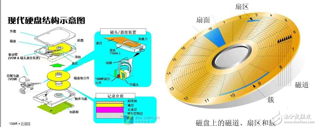
Relative to the CPU, the internal storage of electronic structures, disk storage is a mechanical structure. The data is written to the magnetic disk by the electromagnetic flow in such a manner that the polarity is changed by the electromagnetic flow, and is read back in the opposite manner. A hard disk is composed of a plurality of disks, and each disk is divided into tracks, sectors, and the smallest unit cluster. Each disk has a head for reading and writing data. The hard disk drive controls the movement of the head.
1.2.5 Virtual Hard Disk (VHD) and Solid State Drive (SSD)
With the development of computers, slow disk speed has become an obstacle to the speed of computers. In most cases, your CPU is fast enough and the memory is large enough, but when you open a program or game, the loading speed is always slow. (The article on the process of loading the program will be discussed later). The reason is that the disk read and write speed is too slow, so there was a virtual hard disk. It is to virtualize a part of the memory into a hard disk, so that some cache files are put directly into memory, which speeds up the process of accessing this data. But his problems are volatile. Of course you can save to disk, but the speed of loading and writing back will increase as the amount of data increases. So this applies to some temporary data, such as browser cache files.
The SSDs have come out in recent years. With the development of technology, the prices are getting cheaper. More and more people use SSD+HHD to build systems and increase the speed of the system. In fact, SSDs were based on DRAM products in the 1980s, but they could not be popularized because of their volatile nature and price. The current SSD uses Flash Memory. The most common SSDs on the market today are SLC, MLC, and TLC storage media. We know Flash is limited to the number of writes. And SLC "MLC" TLC. The current mainstream SSDs use MLC, such as Intel 520 and Samsung 830 series. Of course, Samsung has also withdrawn from TLC-based SSDs, and the price is relatively cheaper.
1.2.6 Remote Storage
Simple can be understood as storing data instructions on other machines, such as distributed systems, Web Service Servers, HTTP Servers, and now hot cloud storage. Computers are connected to each other over the network. Compared to disk, the speed of remote storage is calculated in seconds.
1.3 Locality
Through the above introduction we have an understanding of computer memory and know that the higher the memory level, the faster. So why do we have to layer the memory? Divided to make up for the difference in the direct speed between CPU and memory. All of this is effective because of one characteristic of the application: locality.
We know that the computer system is a stored program that executes sequentially. Therefore, when executing a program instruction, the instruction following it is likely to be executed in the next instruction cycle. After a storage area is accessed, it may be accessed again in the next operation. This is the two forms of locality:
Time locality
Spatial locality
For modern computers, we use locality at all levels of applications, operating systems, and hardware.
Hardware: The speed of access to main memory is increased by introducing cache memory to store recently accessed instruction data.
Operating System: Allows caching of blocks that use main memory as a reference block for virtual address space and blocks from disk files.
Applications: Cache some remote services such as HTTP Server's HTML pages on the disk of this degree.
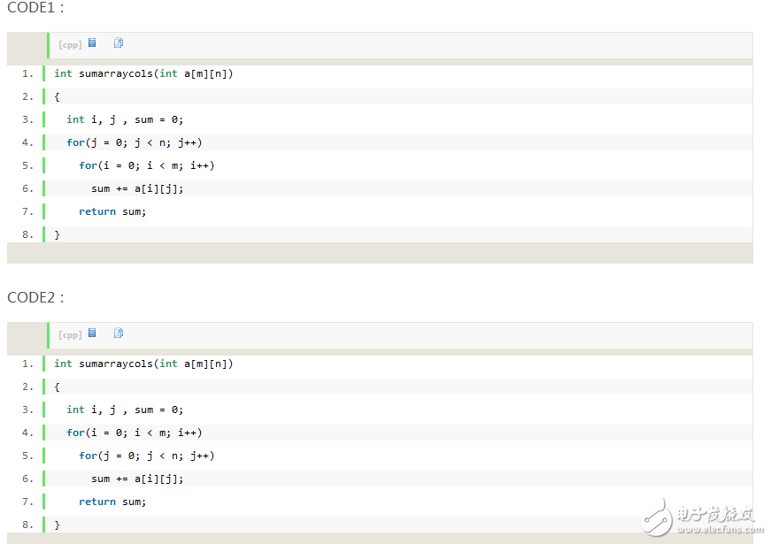
The above two code differences are only for the order of the for loop, but the locality is a lot different. We know that arrays are stored in memory in the order of the rows. However, CODE1 does access by column, which may result in cache misses (required data is not in the cache, because Cache stores continuous memory data, and CODE1 access is not linked), which reduces program execution. speed.
2 memory access and bus
The storage technology and layering of the memory have been introduced in the foregoing, and the CPU has also been mentioned to acquire data and instructions from the memory. This section describes how the CPU and the memory communicate with each other.
2.1 Bus
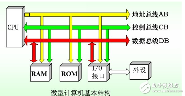
The so-called bus is a common communication trunk for transmitting information between various functional components. It is a transmission harness composed of wires. We know that computers have five components: the calculator, the controller, the memory, and the input and output devices, so the bus is the wire that connects these components.
According to the type of information transmitted by the computer, the bus of the computer can be divided into
Data bus: The data bus DB is a bidirectional tri-state bus, ie it can transfer data from the CPU to other components such as memory or input/output interfaces, as well as transfer data from other components to the CPU. The number of bits in the data bus is an important indicator of the microcomputer and is usually consistent with the word length of the microprocessor. The 32-bit, 64-bit computer we are talking about is the data bus.
Address bus: The address bus AB is used to transfer addresses. Since the address can only be transferred from the CPU to the external memory or I/O port, the address bus is always unidirectional and tristate, which is different from the data bus. The number of bits in the address bus determines the amount of memory that the CPU can directly address.
Control bus: The control bus is mainly used to transmit control signals and timing signals. The transmission direction of the control bus is determined by the specific control signal, which is generally bi-directional. The number of control buses depends on the actual control requirements of the system. In fact, the data bus and the control bus can be shared.
The bus can also be classified according to the inside and outside of the CPU:
Internal bus: Inside the CPU, the bus used to transfer data between registers and between the arithmetic logic unit ALU and the control unit is called the internal bus.
External bus: The external bus, commonly referred to as a bus finger, is the communication path between the CPU and memory RAM, ROM, and input/output device interfaces. It is also called the system bus.
2.2 Control chip
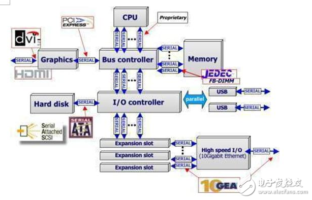
In front of me, I introduced the classification of the bus in our simple model. The CPU communicates directly between the bus and the memory. In fact, in a modern computer, there is a module that controls the chip. The CPU needs to interact with memory, I/O devices, etc. There will be a variety of control chips with different functions, which we call the control chipset (Chipset).
For the current computer architecture, the control chip is integrated on the main board, typically a North-South bridge structure and a single-chip structure. The bus connected to the chip can be divided into a front-side bus (FSB), a memory bus, an IQ bus, an expansion bus, and the like.
North and South Bridge chip structure:
Northbridge chip, which controls the type of CPU, motherboard bus frequency, memory controller, display core and so on. It is directly connected to the CPU, memory, graphics card, Southbridge, so it has a very large amount of data;
Front-side bus: A bus that connects the CPU to the North Bridge chip. The FSB frequency refers to the speed of data exchange between the CPU and Northbridge. The faster the speed, the higher the data bandwidth, the better the computer performance;
Memory bus: A bus that connects memory to the North Bridge chip. Used for communication with Northbridge;
Graphics bus: The total new card that connects the graphics card to the Northbridge. There are currently AGP, PCI-E and other interfaces. In fact, there is no video card bus, generally considered to belong to the I / O bus;
South Bridge chip, which is mainly responsible for the external interface and internal CPU connections;
I/O bus: connects the external I/O device to the bus of Southbridge, such as USB device, ATA, SATA device, and some expansion interfaces;
Expansion bus: Mainly PCI, ISA and other slots provided on the motherboard;
Single chip structure: The single chipset is mainly to cancel the Northbridge, because now the CPU has a built-in memory controller and does not need to be controlled through the Northbridge. This can increase the frequency of the memory controller and reduce the delay. And now some CPUs also integrate display units. It also makes the display chip more frequent and less delayed.
2.3 Operating frequency
Data bandwidth = (bus frequency * data width) / 8
2.3.1 FSB
FSB is based on the vibration speed of digital pulse signals. It is the speed at which the CPU operates with the system bus and other external devices. We know that there is a timing generator in the computer to ensure that all components work together, and the external frequency mentioned here is the frequency of this timing generator. FSB is also the operating frequency of the system bus.
2.3.2 Frequency and Control Chip
At the beginning of the computer, the CPU and memory I/O settings are directly connected through the bus without the control chip. All devices work synchronously on the same bus frequency.
However, with the development of the CPU, the CPU speed is increasing. However, it is limited by I/O devices. So there is a chip. He makes the I/O bus not directly connected to the system bus of the CPU. In this way, there are two buses with different frequencies. This chip actually acts as a down-converter, which is also a frequency division technique with respect to the system bus.
However, the CPU speed has evolved quite rapidly, and the speed of the CPU has been higher than the speed of memory operation, so the concept of frequency multiplication has been introduced. The CPU operates at a higher frequency without changing the FSB and system bus frequency.
Later on, Northbridge chips appeared, and the bus before the CPU and Northbridge was called the FSB bus, and the memory and Northbridge were previously called the memory bus.
2.3.2 Frequency division and frequency multiplication
Frequency division: Makes I/O devices work with higher FSBs. For example AGP, PCI bus, running frequency is 66MHZ and 33MHZ, so for a 100MHZ FSB, using 2/3 or 1/3 frequency division way can make CPU and peripheral device work synchronously. Otherwise the device may not work properly.
Frequency Multiplication: In order to increase the CPU frequency and normal work with memory, frequency multiplication occurs. So for the CPU, his actual frequency is the FSB* multiplier.
2.3.3 FSB frequency
Earlier we now know that CPU and Northbridge connections are via FSB. The FSB frequency indicates the operating speed between the CPU and the Northbridge. But from the front we know that the actual frequency of the FSB is the same as the FSB. However, with the development of technology, Intel's QDR technology and AMD's HT technology enable the CPU to transmit data 4 times in one clock cycle. Therefore, although the frequency of the FSB is said to be at the frequency of the early FSB, the equivalent frequency is 4 times the frequency. So we say that the FSB frequency is the equivalent frequency, not the actual operating frequency. With the development of technology, the FSB of Intel chips has 800MHz, 1600HMz and so on. However, with the disappearance of the Northbridge chip, the probability of FSB is slowly going away.
2.3.4 Memory Frequency
For the memory frequency we can see that it generally includes the core frequency, bus frequency and transmission frequency:
Similar to the FSB, the core frequency is based on the pulse oscillation signal.
The bus frequency refers to the operating frequency of the memory bus. This is the frequency of operation between the memory and the Northbridge.
The transmission frequency is similar to FSB, which refers to the frequency of actual data transmission.
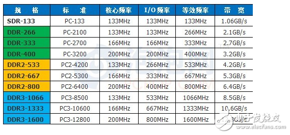
For SDR, its three frequencies are the same. DDR can transmit 2 times of data in one clock cycle, so its transmission frequency is 2 times that of the core and bus frequency. DDR2 uses 4-bit read-ahead on the basis of DDR, so the bus frequency is twice the core frequency, while DDR3 uses 8-bit pre-reading, and the bus frequency is 4 times the core frequency.
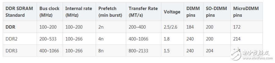
We can see from the table below. So we often say that DDR3 1600, DDR2 800 refers to the memory transmission frequency. The same technology is also available for graphics cards such as AGP4X, 8X, PCIE-8X, and 16X.
With the FSB speed accelerating, the memory bus frequency has become a bottleneck, so there are DDR dual channels, dual channel refers to the chip has two memory controllers, so you can make the transfer rate doubled.
2.3.5 Memory Bus Operation
Because the frequency of the memory bus is different, there are two synchronous and asynchronous working modes between the memory and the CPU.
Synchronous mode: The memory bus frequency is the same as the CPU FSB. Like the previous PC133 and P3 processors, they work in synchrony at 133 MHz. And when you are overclocking you need to have a higher bus frequency memory. Of course, we also need the support of the Northbridge chip.
Asynchronous mode: The memory bus frequency is different from the CPU FSB. With the increase in CPU FSB sleep, the memory must also be updated, so there is an asynchronous way. For example, the P4 CPU has a FSB of 200 MHz, but the memory can use DDR333 to run. At the same time asynchronous mode is often used when overclocking. In general there will be a memory asynchronous ratio. There will be corresponding options in the BIOS.
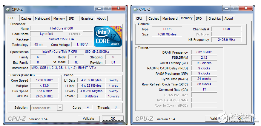
In terms of performance, the delay in the synchronous mode is better than that in the asynchronous mode. This is why it was said that the CPU of the P4 200 FSB should use DDR400 in order to maximize its effectiveness. But this is not absolute. For example, the CPU FSB of my I5 processor works at 100MHz, and the bus frequency of the DDR3-1600 I use is 200MHz. Although it is not synchronized, it has a higher transmission rate. So you can't generalize.
2.3.6 QPI and HT Bus Technology
From the front we know that the FSB has a great impact on the performance of the entire system. The data bandwidth of the 1600 MHz FSB can only provide 12.8 GB/s. So with the development of technology, the latest computers are now basically single-chip designs. The functions are integrated inside the CPU. So the FSB that we said earlier does not exist. For Intel and AMD, the two major chip manufacturers have their own technologies to increase the transfer rate between the CPU and memory and other devices to meet higher computing requirements.
QPI: Intel's QuickPath Interconnect technology is abbreviated as QPI, translated as Fast Channel Interconnect. Used to implement direct interconnection between chips, rather than connecting to Northbridge via FSB. The early 20-bit wide QPI connection has an amazing 25.6GB/s bandwidth, which is far from comparable to FSB. With the development of technology, the peak value can reach 96GB/s in the high-end Itanium processing.
HT: The HyperTransport essence is an end-to-end bus technology designed for the interconnection of integrated circuits on the main board. The purpose is to speed up the data transmission speed between chips. After HyperTransport technology is used on the AMD platform, it refers to the connection bus between the AMD CPU and the motherboard chip (if the motherboard chipset is a north-south bridge architecture, it refers to the CPU to the northbridge), ie, the HT bus. HT3.1 theoretically can reach 51.2GB/s.
In addition, the QPI and HT transfers in the chip do not need to go through the North Bridge new chip. In addition to the integrated memory controller in the CPU memory, the graphics core of the PCI-E2.0 can be integrated unexpectedly, making the integrated graphics core frequency and data throughput. A substantial increase.
As shown in the figure, the Core I7 processor's FSB is only 133MHz. After using QPI technology, the bus frequency reaches 2.4GMhz, while using DDR3-1600 memory, the memory bus frequency is 800MHz.
2.3.7 Summary
This conclusion describes the computer bus system and the interaction between the CPU and various devices. We can see that in addition to the speed of the CPU itself, the speed of the bus also affects the overall performance of the computer. From the perspective of the development process, the bus is also a process of division and integration. From the initial bus, to the later separate I/O bus, memory bus, is to improve CPU efficiency. When the CPU and memory speeds have reached a certain stage, DDR and dual-channel technologies have emerged, which have improved the transmission rate without increasing the core frequency. Then there was a case where the direct bus communication between the CPU and the memory reduced the delay. (I have been in touch with computer DIY since 2000 and graduated in 2007. I am very interested in DIY. However, as computers are getting faster and faster, I am still not sure about them. It takes me a lot of time to review these knowledge.)
3. I/O device
The front part mainly introduces the communication between the system bus and CPU and memory. The last part briefly introduces how the CPU and I/O devices communicate. For computers, input and output devices are also five major components. We know that the operating frequency of I/O devices is much slower than that of the CPU. For example, the early PCI interface operating frequency was only 33MHz, and the hard disk IDE-ATA6 transmission rate was only 133MB/s. The current SATA3 interface speed can reach 600MB/s.
3.1 Principles of I/O Devices
For hardware engineers, I/O devices are physical devices composed of electronic chips, wires, power supplies, electronic control devices, and motors. For programmers, the only concern is the programming interface of the I/O device.
3.1.1 I/O Device Classification
Block devices: Block devices store information in fixed-size blocks. Each block has its own address and is addressable independently of other blocks. Such as disk, USB flash memory, CD-ROM and so on.
Symbol device: A character device receives or sends a character stream in units of characters, and the character device cannot address it. Including printers, network cards, mouse and keyboards, etc.
3.1.2 Device Controller
I/O devices generally consist of two parts: mechanical parts and electronic parts. Electronic devices are generally called device controllers. They usually appear in the form of a chip on a computer, such as the South Bridge chip we introduced earlier. Different controllers can control different devices. So the South Bridge chip contains a variety of device controllers, such as hard disk controllers, USB controllers, network cards, sound card controllers, and so on. The connection to the device itself is provided through the bus and the card slot. Such as PCI, PCI-E, SATA, USB and so on.
3.1.3 Drivers
For different device controllers, the operational control is different. So he needs special software to control him. The role of this software is to specifically talk to the device controller. This software is called the driver. In general, the driver is provided by the hardware vendor. So we sometimes encounter situations where some devices cannot be used because there is no driver installed. The current OS always contains a large number of generic drivers, so that we do not need to install additional drivers after installing the system. However, the universal driver can only use the basic functions of the device.
Since the driver is developed by a non-operating system vendor and needs to be installed into the operating system and called, a unified model is needed to develop the driver. Otherwise, the operating system cannot operate all kinds of devices. In the foregoing, we know that devices are not classified into two categories, so the general operating system defines the standard interfaces of these two types of devices.
3.1.4 Memory-Mapped I/O
Each controller has several registers and CPUs to communicate with. By writing these registers, you can instruct the device to send or receive data, turn it on or off. The status of the device can be known by reading these registers. Because of the limited number and size of registers, devices typically have a buffer of RAM to hold some data. Such as hard disk read and write cache, graphics memory and so on. On the one hand to provide data storage, on the one hand is to improve the speed of I / O operations.
The question now is how does the CPU communicate with the registers or data buffers of these devices? There are two alternatives:
Each controller is assigned an I/O port number, and all controllers can form an I/O port space. Stored in memory. General programs cannot access, and the OS reads or writes data from the device through special instructions and port numbers. Early computers were basically this way.
All controller registers are mapped into memory space, so each device's register has a unique address. This is called memory-mapped I/O.
The other way is a combination of the two, the registers have I/O ports, and the data buffers are mapped to memory space. PenTInum uses this method, so in IBM-PC compatible machines, 0-640K of memory is the I/O port address, and the address of 640K-1M is reserved for the device data buffer. (About the memory distribution later article will introduce)
For our programmers these two programs are different
The first method requires the use of assembly language, while the second method can be programmed using C language, because he does not require special instruction control, and the I/O device and other normal data access methods are the same.
For the I/O mapping method, no special protection mechanism is needed to organize access to the I/O, because the OS has already completed this part of the work and will not allocate this segment of memory addresses to other programs.
The instructions available for memory can also be used on the device's registers.
Any technology has a bit of a drawback, as does the I/O memory map:
As mentioned earlier, Cache can cache memory, but there is a problem if you cache the I/O mapped address space. So there must be a mechanism to disable the I/O mapping space cache, which increases the complexity of the OS.
Another problem is that because they need to determine whether they are memory or I/O operations after sending an instruction, they need to be able to check the entire memory space. Previously, the CPU, memory, and I/O devices were on the same bus, so checking was convenient. However, in order to improve CPU and memory efficiency, there is a high-speed bus (such as QPI) between the CPU and memory. In this way, the I/O device cannot view the memory address because the memory address bus sideways falls on the high-speed bus of the memory and the CPU, so an extra chip is required to handle (the role of the North Bridge chip and the memory controller), which increases the complexity of the system. degree.
3.2 CPU and I/O device data exchange
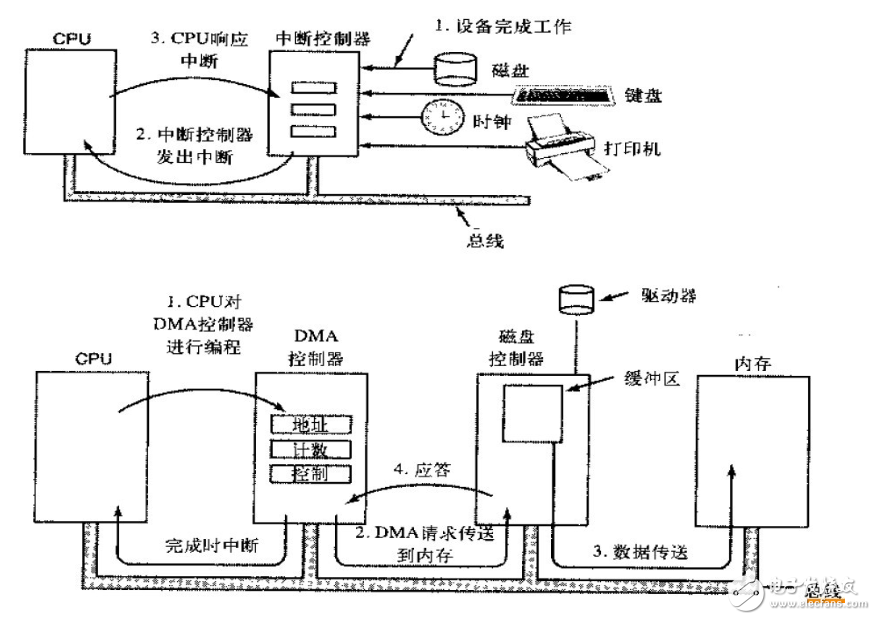
It is known in the past that the CPU exchanges data with the I/O device by means of memory mapping. However, for the CPU, whether it is reading data from the memory or the I/O device, it is necessary to put the address on the address bus and then control the CPU. The bus passes a READ signal and also uses a signal line to indicate whether it is reading data from memory or I/O. Because the memory area for I/O mapping is specific, there is no indistinguishable memory or I/O operation. There are currently 3 ways to operate:
Program Control I/O: After the CPU issues an instruction to the I/O device, it checks the I/O device to complete the work through a program inquiry method. If it finishes, it reads the data. The disadvantage of this method is that the CPU is working on the I/O device. Occupied.
Interrupt Drive I/O: The CPU is a scarce resource, so in order to improve utilization, reduce I/O waiting. When the I/O device is working, the CPU does not wait any longer, but performs other operations. After the I/O device is completed, the CPU is notified by a hardware interrupt signal. The CPU is working on the following tasks, such as reading data into memory. However, only one byte can be requested at a time, which is inefficient.
DMA: Direct Memory Access utilizes a feature of the chip that exists between the CPU and the I/O device. When the CPU needs to operate the I/O device, it only needs to send a message to the DMA chip. All subsequent things are completed by the DMA. When the required data is put into memory, the CPU is notified to operate. The entire process directly deals with the memory bus. The CPU also only needs to interact with the DMA chip and memory, which greatly increases the speed.
to sum up
This article describes the classification and working principle of the memory in the computer components, as well as the way I/O settings work. Connect the various components via the bus. We can see that the development of the computer is not only the development of CPU, memory and I/O devices, but also the bus has played a very key role. Through the introduction of the first two chapters, you should have a general understanding of the working principle of computer hardware. Later, it will mainly focus on the operating mode of computer operating system software. Of course, these are also inseparable from the characteristics of some hardware.
Every year, our Hengstar company will display all the latest new products at online large-scale trade shows, hoping to arouse the interest of distributors, dealers and potential customers. New projects are our company's continuous improvement of existing products or the launch of the latest "new" models. New products are the design and development of all new products that many people have not seen or even thought of. Introduce products that consumers want. New Product Introduction (NPI) helps to bring all the right resources together at the right time.
New product display,digital signage monitors,all in one pc,touch screen pc,smart home tablets,open frame touch screen monitor
Shenzhen Hengstar Technology Co., Ltd. , https://www.angeltondal.com