Let the sensor handle the noise and nonlinear response generated by any color channel from nine aspects
The core of a typical image sensor is a CCD unit (charge-coupled device) or a standard CMOS unit (complementary metal oxide semiconductor). CCD and CMOS sensors have similar characteristics and are widely used in commercial cameras. However, most modern sensors use CMOS cells, mainly for manufacturing reasons. Sensors and optics are often integrated to make wafer-level cameras that are used in areas such as biology or microscopy, as shown in Figure 1.
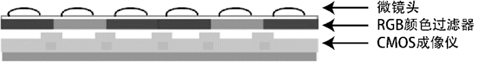
Figure 1: Common arrangement of image sensors incorporating optics and color filters
Image sensors are designed to meet the specific goals of different applications and offer different levels of sensitivity and quality. To get familiar with the various sensors, check out their manufacturer information. For example, to have the best compromise between silicon-based modes and dynamic response (for achieving light intensity and color detection), the size and composition of each photodiode sensor unit needs to be optimized for a particular semiconductor manufacturing process. ingredient.
For computer vision, the effect of sampling theory is important, such as the Nyquist frequency used in the pixel range of the target scene. The sensor resolution and optics together provide enough resolution for each pixel to image the feature of interest, so there is a conclusion that the sampling (or imaging) frequency of the feature of interest should be an important pixel (for interested In terms of features, it is twice the smallest pixel size. Of course, twice the oversampling is only a minimum target for imaging accuracy, and in practical applications, it is not easy to determine the characteristics of a single pixel width.
For the best application, to get the best results, the camera system needs to be calibrated to determine the pixel noise and dynamic range of the pixel depth under different illumination and distance conditions. In order to be able to handle the noise and nonlinear response of the sensor to any color channel, and to detect and correct pixel artifacts, and to model geometric distortion, a suitable sensor approach needs to be developed. If you use the test mode to design a simple calibration method, this method has a fine-to-thick gradient in terms of grayscale, color, feature pixel size, etc., and you will see the result.
1, sensor material
Silicon image sensors are the most widely used, and of course other materials are used, such as gallium (Ga) to cover longer infrared wavelengths than silicon in industrial and military applications. The resolution of the image sensor will vary from camera to camera. From single-pixel phototransistor cameras (which use 1D linear scan arrays for industrial applications) to two-dimensional rectangular arrays on ordinary cameras (all paths to spherical arrays are used for high-resolution imaging), it is possible to use . (The sensor configuration and camera configuration are described at the end of this chapter).
Ordinary imaging sensors are manufactured using CCD, CMOS, BSI, and Foveon methods. The silicon image sensor has a nonlinear spectral response curve that is well perceived by the near-infrared portion of the spectrum, but not well for the blue, purple, and near-ultraviolet portions (see Figure 2).
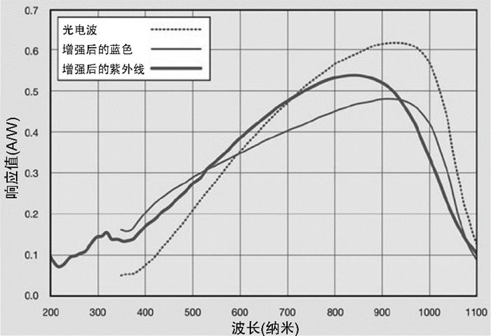
Figure 2: Typical spectral response of several silicon photodiodes. It can be noted that the photodiode has high sensitivity in the near-infrared range around 900 nm, and has nonlinear sensitivity in the visible range across 400 nm to 700 nm. Due to the standard silicon response, removing the IR filter from the camera increases the sensitivity of the near infrared. (The use of spectral data images has been approved by OSI Optoelectronics Co., Ltd.)
Note that when the raw data is read in and the data is discretized into digital pixels, it causes a silicon spectral response. The sensor manufacturer has made design compensation in this area. However, when calibrating the camera system according to the application and designing the sensor processing method, the color response of the sensor should be considered.
2, sensor photodiode components
The key to an image sensor is the size of the photodiode or the size of the component. The number of photons captured by sensor elements using small photodiodes is not as large as using large photodiodes. If the component size is smaller than the visible wavelength of visible light (such as blue light with a length of 400 nm), other problems must be overcome in the sensor design in order to correct the image color. Sensor manufacturers spend a lot of effort to design optimized component sizes to ensure that all colors are equally imaged (see Figure 3). In extreme cases, small sensors may be more sensitive to noise due to the lack of accumulated photons and sensor readout noise. If the diode sensor element is too large, the particle size and cost of the silicon material will increase, which has no advantage. Typical commercial sensor devices have sensor elements that are at least 1 square micron in size and will vary from manufacturer to manufacturer, but there are some tradeoffs to meet certain special needs.
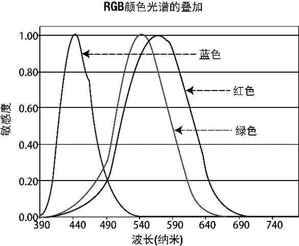
Figure 3: Wavelength assignment of the basic color. Note that the basic color areas overlap each other, and green is a good monochrome alternative for all colors.
3. Sensor configuration: Mosaic, Faveon and BSI
Figure 4 shows the different on-chip configurations of a multispectral sensor design, including mosaic and stacking methods. In the mosaic method, a color filter is mounted on the mosaic mode of each component. The Faveon sensor stacking method relies on the deep penetration of the color wavelength into the physical composition of the semiconductor material, where each color infiltrates the silicon material to varying degrees to image the respective color. The entire component size is available for all colors, so there is no need to configure components for each color separately.
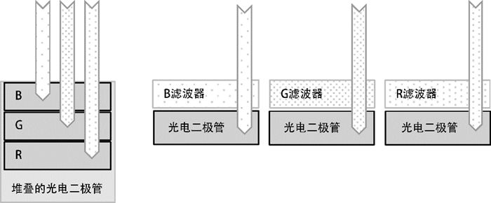
Figure 4: (Left) Foveon method for stacking RGB components: RGB color at each component position and absorbing different wavelengths at different depths; (right) Standard mosaic components: placed on top of each photodiode An RGB filter, each filter only allows a specific wavelength to pass through each photodiode
Back-side illuminated (BSI) sensor structures have larger component areas, and each component collects more photons, thus rearranging sensor wiring on the die.
The arrangement of the sensor elements also affects the color response. For example, Figure 5 shows a different arrangement of basic color (R, G, B) sensors and white sensors, where the white sensor (W) has a very sharp or achromatic color filter. The arrangement of the sensors takes into account a range of pixel processing, such as in the processing of a pixel information by the sensor, combining pixels selected in different configurations of adjacent elements that optimize color response or spatial color resolution. In fact, some applications use only raw sensor data and perform common processing to enhance resolution or construct other color mixtures.
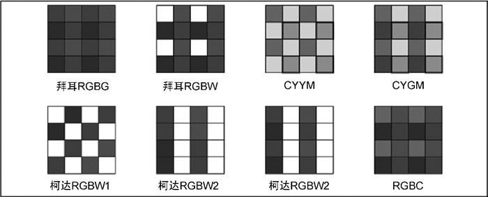
Figure 5: Several different mosaic configurations of component colors, including white, basic RGB colors, and secondary CYM components. Each configuration provides a different approach to optimizing color or spatial resolution for sensor processing (images are from Building Intelligent Systems and licensed by Intel Press).
The size of the entire sensor also determines the size of the lens. In general, the larger the lens, the more light it passes, so larger cameras can be better suited for digital cameras for photographic applications. In addition, the aspect ratio of the elements arranged on the particles determines the geometry of the pixels. For example, the aspect ratios of 4:3 and 3:2 are used for digital cameras and 35 mm film, respectively. The details of the sensor configuration are worth understanding by the reader so that the best sensor processing and image pre-processing can be designed.
4, dynamic range and noise
Currently, the most advanced sensors can provide at least 8 bits per color unit, typically 12 to 14 bits. Sensor components require space and time to collect photons, so smaller components must be carefully designed to avoid problems. Noise can come from the optics used, color filters, sensor components, gain and A/D converters, post-processing or compression methods. The readout noise of the sensor also affects the actual resolution because each pixel unit is read from the sensor and passed to the A/D converter to form rows and columns in digital form for pixel conversion. The better the sensor, the less noise it will produce and the more efficient bit resolution. Ibenthal's work is a good source of noise reduction.
In addition, sensor photon absorption will vary for each color, and there may be some problems with blue, which is the most difficult color for smaller sensor imaging. In some cases, manufacturers will try to build a simple gamma curve correction method for each color in the sensor, but this method is not worth promoting. In applications where color is required, color device models and color management can be considered, and even each color channel of the sensor has non-linear characteristics and a series of simple Lookup Table (LUT) conversions are established.
5, sensor processing
Sensor processing is used to de-mosatheize and condense pixels from the sensor array, as well as to correct for perception. In this section we will discuss the basics of sensor processing.
There is usually a proprietary sensor processor in each imaging system, including a fast HW sensor interface, an optimized very long instruction word (VLIW), and single instruction multiple data (single instruction multiple data). SIMD) instructions and hardware modules with fixed functions are designed to solve the workload caused by massively parallel pixel processing. Typically, the sensor processing is transparent and automated, and is set by the manufacturer of the imaging system, and all images from the sensor are processed in the same way. There are other ways to provide raw data that allows for custom sensor processing for the application, just like digital photography.
6, go to the mosaic
Depending on the sensor component configuration (as shown in Figure 5), the raw sensor data can be generated using the various demosaicing algorithms to produce the final RGB pixels. Losson & Yang and Li et al. gave two very good review articles, which introduced various methods and challenges.
One of the main challenges of demosaicing is pixel interpolation, which combines the color channels of adjacent cells into a single pixel. This is an important issue given the geometry of the sensor element arrangement and the aspect ratio of the cell arrangement. A related problem is the weighting of the color cells, such as how much each color should be in each RGB pixel. Because in a mosaic sensor, the spatial component resolution is greater than the final combined RGB pixel resolution, some applications require raw sensor data in order to utilize all of the precision and resolution as much as possible, or some processing may require enhanced effective pixel resolution. Either need to achieve space-accurate color processing and demosaicing better.
7, correction of bad pixels
Like LCD monitors, sensors can also have bad pixels. By providing bad pixel coordinates that need to be corrected in the camera module or driver, the supplier can calibrate the sensor at the factory and provide a sensor defect map for known defects. In some cases, adaptive defect correction methods are used on the sensor to monitor adjacent pixels to detect defects and then correct for a range of defect types, such as single pixel defects, column or row defects, and similar 2×2 Or 3 × 3 block defects. In order to find defects in real time, the camera driver can also provide adaptive defect analysis, and a special compensation control may be provided in the camera's boot menu.
8, color and lighting correction
Color correction is necessary to balance the overall color accuracy and white balance. As shown in Figure 1-2, the silicon sensor is usually sensitive to red and green colors, but not blue, so understanding and calibrating the sensor is the basic job of getting the most accurate color.
Most image sensor processors include a geometry processor for halo correction, which appears to be darker at the edges of the image. The correction is based on the geometric warping function, which can be considered to increase the illumination towards the edge, which needs to be calibrated at the factory to match the optical halo pattern.
9, geometric correction
The lens may have geometric differences or distortion towards the edges, producing an image of radial distortion. To address lens distortion, most imaging systems have dedicated sensor processors with a hardware-accelerated digital distortion component similar to the texture sampler on the GPU. The geometry corrections for the optics are calibrated and programmed at the factory.
Canaan is a leading provider of supercomputing solutions, distinguished for superior cost-efficiencies and performance. In addressing the limitations of today`s computing hardware, Canaan strives to advance the world we live in by powering transformative technologies.
Canaan is renowned for having invented the world`s first ASIC-powered Bitcoin Mining Machine in 2013, radically catalysing the growth of a computationally-advanced bitcoin mining sector.
Developed through academic research, rigorous expertise in semiconductor design, and backed by a robust network of strategic partners, Canaan continues to expand its suite of advanced hardware offerings, exploring opportunities across some of the world`s most exciting emerging technologies.
Canaan AvalonMiner:Canaan AvalonMiner 821,Canaan AvalonMiner 841,Canaan AvalonMiner 741,Canaan AvalonMiner 1246,Canaan AvalonMiner 921,Canaan AvalonMiner 1166 Pro
Canaan Avalonminer,1166 Pro 66T,Avalon 821,Avalon 1246,avalon miner
Shenzhen YLHM Technology Co., Ltd. , https://www.ylhm-tech.com